2026-05-30 01:00:48

Elliot Williams is out where the deer and the antelope play for the next week, so it’s up to Tom Nardi and Al Williams to wrangle this episode of the Hackaday Podcast. They’ll start off by reading some listener messages before talking about the slow extinction of time broadcasts, Linux on cheap smartphones, microcontroller VPNs, and the computers of Spacelab.
You’ll also hear about using a video game’s “Photo Mode” to capture 3D imagery, strange red lights in deep space, and ASCII fish that you don’t need to feed. The episode wraps up with a discussion of WWII spy tech and the revelation that modern smartphones and powerful magnets don’t always mix.
Check out the links if you want to follow along, and as always, tell us what you think about this episode in the comments!
Direct download in DRM-free MP3.
2026-05-29 23:30:14
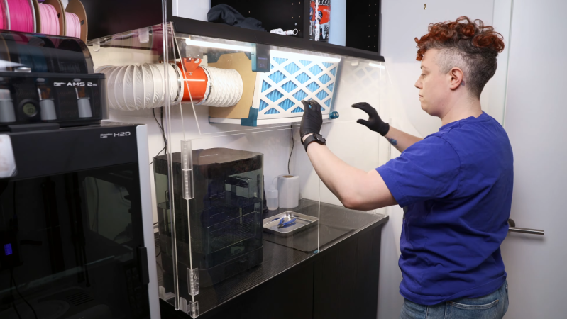
For a certain kind of intricate, highly-detailed manufacturing, there’s really no substitute for a resin 3D printer, and it’s therefore unfortunate that they require so many poisonous chemicals. The resin itself usually contains irritating acrylates and methacrylates, it can emit a wide spectrum of volatile organic compounds (VOCs) during printing, and even the isopropyl alcohol used in cleaning is moderately toxic. [Allie Katz] accordingly built this fume-control enclosure for resin printing and other ventilation-critical processes.
The biggest constraint was space: [Allie]’s workspace had a fairly limited volume available, and the enclosure needed to hold an SLA printer, an isopropyl alcohol washing station, a UV curing chamber, and miscellaneous supplies. Most of the enclosure was made out of IKEA cabinets, using some large cabinets at the base to hold the printer and curing station, a countertop over these to hold the washing station, and more cabinets above to hold supplies. An MDF backing panel and acrylic side panels enclose the workspace between the cabinets. There was no safe way to exhaust fumes, so the enclosure recycles its air: a fan pulls air in through an activated-carbon filter mounted above the work area and into the plenum behind the chamber, from which it passes through the printer’s cabinet back into the workspace enclosure. Panel filters surround the carbon filter to catch particulate matter.
The enclosure uses four ESP32-based boards for automation: one uses a touchscreen to display data, and three are paired with BME680 sensors, primarily to report VOC concentrations. One, which also has a particulate matter sensor, senses air quality in the main chamber and plenum, one monitors air quality in the rest of the shop, and the third detects clogging from within the filter enclosure. The first real test of the chamber was to 3D print and paint some handles for the cabinets. It worked as expected, detecting the increased VOCs and ramping up the fan to keep them in check.
We’ve seen a ventilated printer enclosure before, that time for an FDM printer. Although their hazards are less blatant, they too can produce dangerous fumes, which could possibly be carcinogenic.
Thanks to [Keith Olson] for the tip!
2026-05-29 22:00:19

Ubiquiti released a new security bulletin detailing fixes for six security issues, including one rated 9.1 (critical) and one scoring a perfect 10.0 on the CVE risk scale.
The vulnerabilities range from path traversal revealing configuration files (escaping from the web server by requesting a path like “../../../../../etc/passwd” for instance), to command injection (running arbitrary shell commands on the system), and actually changing device configurations. Some of the reported vulnerabilities require an account on the management server, but some only require network access .
Fortunately, all of the vulnerabilities require access to the network in the first place to exploit – but this could include access to open guest networks as well as trusted users. If you run Ubiquti or UniFi equipment, chances are the automatic update function has already integrated the fixes, but make sure to check the advisory to see if you’re impacted and update accordingly!
FatGid lets FreeBSD join the fun of kernel exploits to gain root.
The FatGid vulnerability doesn’t require any manipulation of disk cache; instead it is a direct kernel stack overflow in a system call. The kernel miscalculates the size of a variable as 8 bytes instead of 4, which when used later interacting with a user buffer allows the stack overflow.
Like the recent spate of Linux local privilege escalation attacks, this requires the attacker to already have an account on the system or the ability to run arbitrary programs, but remember that any bug in network services which allows command execution gets you there, so if you run network exposed FreeBSD, it’s time to update!
Phishing-as-a-service platforms have been gaining traction, allowing criminals to automate targeting users with crafted lures. The FBI has issued a warning about the Kali365 service in particular.
Kali365 targets credentials for Microsoft 365 accounts by directing users to the official Microsoft portal for linking additional devices to the account, attaching an attacker device directly to the user identity. Alternatively, the framework steals credentials by directing the user through a hostile service which presents a false login page which captures browser sessions along with authentication cookies and tokens once the user answers the fake multi-factor login prompts.
Automating the phishing process lowers the bar for the skill level needed to create authentic-looking lures and makes it simpler for criminal groups to attack large numbers of users; Phishing-as-a-service groups operate as companies offering customer support, tracking dashboards, and pre-made phishing templates.
CrowdStrike, Google, and the ShadowServer Foundation have done a coordinated takedown of the infrastructure used by the Glassworm supply-chain botnet.
Glassworm has been mentioned previously; it is one of several major worms infecting the open source package supply chain repositories like NPM and PyPi or the Visual Studio extension repository. Once a victim installs a compromised package or extension, the Glassworm trojan steals any saved authentication tokens for package repositories, GitHub accounts, AI services, and any SSH keys found, and begins the stage two infection. Using the stolen credentials, the worm infects any GitHub workflows, packages, and extensions the user has access to, and installs a remote-access trojan which waits for further commands.
Glassworm used a complex control server structure including blockchain memos, BitTorrent files, and public Google Calendar entries, but the coalition of companies was able to interrupt all control channels simultaneously. Hard-coded aspects of the worm will continue to function, but all behavior which requires downloading payloads from the control servers has been disrupted.
This isn’t the first time multiple Internet companies have coordinated to take down malware, but it’s always good to see action against threats which have been decimating the package repository infrastructure lately.
On the positive side of things, TechCrunch has an article about modern features to protect users against spyware. If this isn’t news to you, there’s still almost certainly someone in your life who will benefit from a user-friendly write up of best practices!
Both major commercial mobile platforms (iOS and Android) offer advanced protection features which are minimally invasive. For users who are likely to be higher targets of spyware like journalists, lawyers, and human rights activists, or simply those who are worried, these features offer real protection.
The features explained in the article include Apple’s Lockdown mode, Androids Advanced protection mode, and WhatsApp specific application settings, all of which work to reduce common attack surfaces for devices. The advanced security modes typically have minor impacts on performance and battery life due to disabling optimization features which introduce additional complexity and attack surfaces (such as just-in-time compilation of JavaScript code into native instructions.). When situations call for an abundance of caution, a few percent of battery life daily is a reasonable compromise.
Go check out the full write up!
An exploit researcher known only as “NightmareEclipse” has been featured here several times in the past months already. Showing intense frustration with their experience with the administrators of the Microsoft security bug bounty program, they have taken to releasing zero-day exploits against Windows, often coinciding with Patch Tuesday (clearly no accident; by releasing a new exploit on the same day as the Microsoft patch set, it’s unlikely to be fixed before the next months Patch Tuesday at the earliest). Previous exploits released by NightmareEclipse include BlueSun and RedHammer (local user to Windows SYSTEM privilege escalation), UnDefend to disable Windows Defender, and YellowKey which unlocks BitLocker drives using a collection of nothing more than magically named files.
Toms Hardware reports that Microsoft has disabled the researchers GitHub accounts (GitHub being owned by Microsoft has long been a point of concern for security researchers who find vulnerabilities in Microsoft products), as well as the actual Microsoft account used by the researcher.
While it’s certainly within the terms of service of Microsoft and GitHub that accounts may be terminated, the optics are particularly poor in this case, given the confusion around the initial interactions which led the researchers original anger. NightmareEclipse has moved their example code repositories to GitLab in the mean time, and promises Microsoft that “I will make sure your bones are shattered on July 14”, implying there will be additional releases (on, you guessed it, what looks like another Patch Tuesday).
Further clouding the issue, an official Microsoft statement indicates they are attempting to bring criminal (not just civil) charges against researchers who do not cooperate with the Microsoft disclosure policies, a stance which will certainly in no way exacerbate the situation.
Dan Goodin at Ars Technica highlights a new paper on fingerprinting users via SSD disk performance, using just standard JavaScript.
The modern web is a hellscape of user tracking, and this attack, dubbed FROST, highlights another technique for identifying unique devices and user patterns based entirely on hardware behavior. By generating a large file using local browser storage via OPFS (origin private file system, an API for JavaScript to create raw files inside the browser storage area) and continually reading and writing data while monitoring the performance, a web page is able to monitor the disk access performance of the device.
Using a neural network trained on timing data, researchers say they are able to determine what apps may be running on the computer alongside the browser – and sometimes even what other websites are being viewed, based solely on the delays in disk IO caused by other applications and websites accessing the SSD. The paper will be presented in July, with researchers saying that the neural network can be trained to recognize “any system which reliably generates SSD accesses”.
Likely, browser developers can mitigate FROST by decreasing the performance of file operations in the OPFS API so that the performance data lacks the fidelity needed to derive user behavior.
FROST is a “side channel attack”; by monitoring one set of characteristics, side channel attacks are able to infer other system behaviors. Side channel attacks can be incredibly subtle and difficult to predict: Another side channel attack method has been to use extremely fine-grained monitoring of the power consumption of a device to derive encryption keys, predicting the CPU instructions and values based on the amount of power used to set the internal registers.
Programming languages have been moving towards stronger default memory models, making programs more secure by default by eliminating behaviors which are commonly exploitable. Using a memory-safe language does not prevent logic errors or other security issues, but can still help by eliminating common mistakes.
Microsoft has posted an extensive article about new enhancements for C# in .NET 11. Borrowing in many ways (that’s a programming joke) from the Rust memory model, C# 16 will add additional memory enforcement and object lifetime, detecting when memory is no longer available and preventing invalid memory accesses on expired objects, with the goal of eliminating use-after-free memory corruption and attacks.
C# 16 will also increase the meaning of the “unsafe” keyword, a mechanism introduced in C# 1.0 and since heavily adopted by newer languages such as Rust and Swift. Code marked as unsafe in C# 16 is able to bypass the stricter memory model, but all code referencing it must also be marked as unsafe. Making unsafe code more difficult to use increases the overall friction of doing things the dangerous way, while clearly marking code which is higher risk.
There are few magic bullets for secure programming, but reducing the ways a programmer can make simple mistakes can be a big win.
2026-05-29 19:00:57
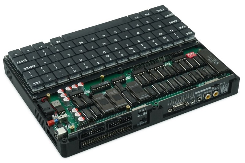
Do you remember, some years ago, when that brand-new 8086-based laptop hit the shelves? Great for PC lovers, but not so fun for those on the fruitier side of the street. Well, the same Chinese firm that brought us the Book8086 are back, this time with an ‘Apple’ Laptop that is decidedly not a MacBook– the Book II is a dual-processor Apple II clone in a laptop form factor.
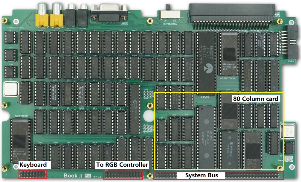
Dual processor? On an Apple II? It wasn’t that uncommon, back in the day — that’s what the Z80 softcard was, after all: a second processor that let you run CP/M and associated business applications, and this one has it built-in. It also has the 80-column video card, a second floppy controller, a printer interface, and a 16 kB ROM card for languages. That leaves two of the Apple’s expansion slots available, one of which is broken out externally on the back of the laptop, along with the printer and floppy ports.
Useful? Probably no more so than the NEC V20-based PC version. Still, those did find buyers and we have no doubt that this new laptop will, too. Especially since with the right expansion card, you might get this machine running DOS as well. Of course if you don’t feel like shelling out the quid or running an emulator, you can always roll your own Apple II on an FPGA.
Thanks to [Stephen Walters] for the tip! We usually steer clear of product announcements like this, but [Stephen] figured we’d be interested in this one since we covered the then-new retro PC versions way back in 2023.
2026-05-29 16:00:59

As anyone who takes medicines regularly will attest to, the days have a tendency to blur together, making it hard to remember if you did something like take that day’s dose or not. There are plenty of products available to help keep track of medication reminders but many are overly complicated, so [Jeroen] built this one which keeps simplicity and usability as its core design principle.
[Jeroen] calls it the MedMinder, and it’s a small, compact, rectangular device with a four-character display meant to sit on a countertop. When it’s time to take a medicine, the display will show that medicine’s four-letter code until the user pushes the single button under the display, signalling that they’ve taken their dose. If many different medications have to be taken at the same time, it displays the first priority until the button is pushed, and then displays whichever one is next after that.
Programming is a little less straightforward, as the medications need to be added to the source code and uploaded to the Arduino that sits at the center of this build, but with the source code available this isn’t too difficult for someone with minimal experience with microcontrollers.
In an idealized world, technology should make our lives simpler or easier, and this small device goes a long way towards helping with that goal. Especially for an important but mundane task that can be surprisingly easy to lose track of. Although we glossed over the accuracy of this device’s clock in this article, we do have a comprehensive guide for selecting the right real-time clock for microcontrollers like this.
2026-05-29 13:00:26

The use of modern microcontrollers as add-on peripherals for 1980s home computers has delivered significant benefits and capabilities unimaginable in the days when those machines were new. A great example come from [Happy Little Diodes], who’s using a Pi Pico based peripheral for a Sinclair ZX Spectrum to provide something that looks far more modern, a hardware minimap for the iconic Spectrum game, Atic Atac.
The ZX expansion port provides all the bus signals from the Z80 microprocessor, and the peripheral uses a latch to capture Spectrum memory writes. Because the game’s operation is well known it can easily watch out for updates to the in-memory variable that contains the game room ID. It’s then a case of drawing the map with the player centered on the room the are in, for a much more 21st century game interface component.
Having been around when both the ZX and this game were new, we like this add-on, a lot. We can imagine it could relatively easily support other games, too.
Haven’t got a Spectrum? Never fear, you can make yourself one!