2026-07-28 03:43:53
Hello you fine Internet folks,
Today we are over AMD's Advancing AI 2026 event to chit chat on their newly revealed CDNA5 architecture with Alan Smith! AMD's Corporate Fellow and Chief Architect for Datacenter GPUs.
Hope y'all enjoy!
The transcript below has been edited for conciseness, readability, and clarifications.
George: So, what do you do here at AMD?
Alan: Yeah. So, I’m a Corporate Fellow of Graphics Architecture at AMD and responsible for Instinct GPU architecture, which we launched today in MI455 and Helios.
George: Starting off, all the way down into the grunt of the engine of MI455. Prior CDNA architectures were based on the GCN architecture, which dates all the way back to Tahiti from I believe 2012, if memory serves, but with CDNA 5, you have now rebased to RDNA. What were some of the considerations for that rebasing of the architecture?
Alan: Yeah, that's a great question. I think there were many, many considerations for making that transition, right? First of all, you know, we wanted to move onto a modern architecture. There were some of the things that we were carrying from the previous GCN architecture, as you mentioned, that we wanted to enhance, including the cache system and also just the execution engine itself, right? So in terms of work scheduling, sequencing of the waves, and even instruction issue and things like this. So there were many things that we wanted to improve.
And so, we knew we wanted to make a big change in the architecture. We wanted to get significant gains in efficiency, and we felt like the opportunity was there for us to bring together what we had done for RDNA, what we wanted to do with CDNA, in order to bring the AMD GPU roadmap more closely together, which gives us then the opportunity for additional optimization in the future that can benefit both.
And one of the reasons we think that’s really important is because AI is everywhere, as you saw in the keynote today. And so, even from gaming and neural rendering and upscaling and all of these things that are now leaning into AI for GPU, even for rendering on the RDNA side, and the things that we’re doing with AI for data center, there’s an opportunity to really bring that together and leverage them on both product lines. So that’s why we wanted to do that.
George: Speaking of two different product lines, I believe last week we published an article on what is effectively MI430. What are the differences in terms of design for HPC versus AI, what design considerations do you have to make at sort of the WGP level for those two different product lines?
Alan: Yeah, great question. I mean, I think not just the WGP level, but the entire SOC level, how do we think about HPC workloads versus AI workloads? They have a lot of similarities, right? They both thrive on high-bandwidth memory, they both need cluster interconnects, they both really enjoy having a high-performance CPU connected to them with a CPU memory system, cache coherency, and all these things. So all of that is already common, right?
And the only thing that's different is the type of numerics that you need for the codes that you're running. And so, the way that we looked at this is we could have included double-precision floating point in the GPU like we've done in the past, or, you know, we could do even better for both if we took advantage of our chiplet architecture and optimized two versions of the compute chiplet: one for traditional simulation with high-precision formats like double-precision floating point, where we really need all of the full IEEE compliance with 64-bit; and then the same thing for the AI workloads, leveraging as highest throughput that we can achieve for both vector operations and the tensor operations for AI.
So having said that, even within the workgroup processor, still many things are in common, right? We need similar bandwidth out of the register file, out of the VGPR. So we're able to leverage all of that, and also all the scheduling, etc. So all of the support hardware within the workgroup processor from the LDS, the caching, the front-end sequencers, all those things, and the SIMDs themselves for the vector ALUs are all shared. And all we really need to do is modulate the number of double-precision units that we implement within the SIMD.
George: Speaking of the SIMDs, previously, a feature or one of the fundamental building blocks of how GCN worked and prior CDNA architectures was that there were four SIMD16 units that were being issued a Wave64 instruction with one instruction per four cycles. With CDNA 5, you have now moved to four SIMD32 units that are being issued one Wave32 per cycle and you have said that you have deprecated Wave64 support. Why did you choose to deprecate Wave64 support considering that RDNA with a similar SIMD setup has Wave64 capabilities?
Alan: Yeah, great question. I think, you know, the way we were looking at it is there’s some additional overhead that we need to carry for Wave64. There are some opportunities to leverage that in some special cases where you can get a little bit of additional efficiency out of issuing a Wave64 on SIMD32. But we felt like the tradeoffs of branch divergence and register pressure and so forth for continuing to keep that capability in most cases, or the common cases from our traces and workload profiling that we’ve done, we think that running in Wave32 almost all the time is a better solution.
And so we were able to, you know, maybe reduce the overhead that you need to carry for Wave64 and deploy that in order to get better common-case performance, and make up for the little bit of optimization that you can get from Wave64 on SIMD32.
George: Okay. So in RDNA 3 and 4, they have four SIMD32 units, but there’s also an extra bank of ALUs per SIMD. Does CDNA 5 have that extra bank of 32 ALUs basically, or is it just 32 ALUs per SIMD?
Alan: Yeah, I think in our SIMDs we have, it’s not always exactly 32 units per lane, right, because in some cases we have more throughput than can be achieved. So we have things like VOP2 instructions...
George: Where you need dual issue?
Alan: Yeah, where you’re effectively doubling the rate, if you will. So you need effectively multiple units per lane in order to get that higher throughput.
George: Speaking of higher throughputs and specifically the register file, with CDNA 5, you have massively increased the amount of VGPRs that a single wave can access: from 256 VGPRs to 1024 VGPRs. Why was that change made?
Alan: The reason we increased the addressing was just to give the waves less register pressure effectively because more of the waves are better able to share more VGPRs.
George: And in terms of the capacity of the register file, it is also 1024 VGPRs in terms of the physical number of registers, which is less than RDNA has. Why fewer in this bigger compute architecture?
Alan: I'll need to go check that.
In a follow-up email, Alan clarified that the VGPR register file size on CDNA5 is sized for the programs that CDNA5 will be used for which has different register file behaviors to what RDNA3/4 will usually run into.
George: On the diagrams it shows a WGP cache of 384 kilobytes and it splits it as 320 and 64 for the LDS and data cache/vector cache whereas some of your LLVM commits show that that number is fungible. So can you change the capacities of the LDS and the vector on the fly, or is that set?
Alan: Yeah. So the architecture was designed to support it to be programmable, but on MI455, we're going to have it as a fixed ratio. We find that for the MI455 deployments, having the larger LDS is almost always the balance that you need for the high tensor throughputs. And so we'll have it always fixed at 320 kilobytes and 64 kilobytes, as you mentioned, for the vector data cache.
George: So then, would MI430 potentially have a different split, or would it be, again, that sort of being able to change on the fly for different workloads?
Alan: It may have a different split.
George: Speaking of caches, that’s a big change specifically at the XCD level. Whereas for CDNA 3 and 4, we had sort of the L1 that was private per CU, then you had the L2 that was per XCD, and then you had the MALL AKA Infinity Cache that acted as sort of the glue to everything, that has changed. Why was that change made?
Alan: Yeah. So there were a couple of reasons that we were addressing with these changes. One of the things that we really wanted to do for MI450 series beyond what we had in 300 and 350 series was die-scope atomics or global atomics. So we wanted to move that back into the L2 cache, where we could get a higher throughput implementation, so that was one of our design goals.
We also wanted to eliminate the kernel boundary flush that we had on the L2 cache that was implemented in the XCD for global visibility on MI350 series. And then we also just wanted to increase the bandwidth for global L2 beyond what would be capable to go across the chip boundaries between the two cache fabric dies.
And so, the way that we did that is we effectively implemented a client-side cache instead of a memory-side cache. So we have these two client-side caches. We used the area that would have been implemented, or would have implemented an Infinity Cache on MI355 on the base die, built a large global L2 cache on each of them, and now all of the shader engines that are in the accelerator complex dies situated on one of those base dies, they all share that L2 cache.
So the last thing that you get the benefit of is from L2 cache data reuse: we get more sharing across more shader engines. So we have eight shader engines now that share a common L2 cache versus what we had on MI300 and 350 series.
And then what we do with those two caches: now each one of them is able to cache all of the memory. So all of the global addresses within the whole GPU, each of them can cache locally. And so those cache accesses don’t have to traverse across the chiplet boundary on the base die, versus on MI300 and 350, where in order to access the capacity of the MALL, the transactions would have to go across longer latency and higher power to go across all of the base die chiplets on the I/O dies.
George: So then, can a WGP on FCD0 access the cache in FCD1?
Alan: They do not.
George: Okay. So what is the bandwidth between the two FCDs?
Alan: We sized the interface between the two FCDs so that we can achieve full memory bandwidth in what we call NPS1. So if you look at the bisectional bandwidth of the two dies, it’s effectively sized relative to the total HBM bandwidth of the device, such that 50% of the bandwidth when you’re sharing from one side to the other... each side needs to access 50% of their accesses on their side and 50% on the other side.
And so that interface is sized so that both sides can do that simultaneously and achieve the full bandwidth of the memory system across the two, plus, as you alluded to, we have some coherency traffic because the Infinity Fabric is maintaining cache coherency between those two GL2 caches. So it’s sized appropriately to handle that traffic in addition to the memory traffic, and then also the I/O traffic that we have coming in from the scale-up and scale-out networks.
In a follow-up email, Alan clarified that the die to die bandwidth is 14 TB/s bi-directional.
George: A way to think of this is like sort of the way that EPYC does its cache coherency, I guess?
Alan: It is very similar. From their L3s. So if you think about the L3 cache implementation on EPYC and the way that that’s implemented, it’s very similar here.
George: Cool. And so we come to the ultimate question. While I usually ask “What is your favorite cheese?”, we already know your favorite cheese! So have you tried any new cheeses as of late?
Alan: (Laughs) Um, yeah, I’m still a fan of cheddar, right?
George: I believe your favorite’s Cabot?
Alan: Cabot is, yeah, what we talked about. But you know what? Since I know that you’re a Tillamook fan... I just want to say that I have been eating a lot of Tillamook ice cream lately!
George: Oh yes! Anyway, thank you so much for sitting down with me.
Alan: Absolutely, George.
2026-07-24 01:37:10
Editor’s Note (7/25/2026): The article has been edited with more information about the L2 behavior along with the bandwidth of the die to die interface.
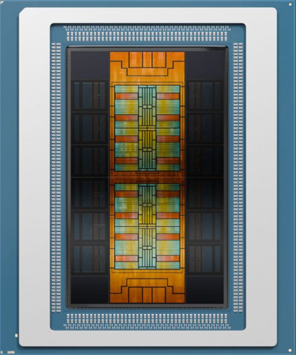
Hello you fine Internet folks, here at AMD’s Advancing AI event we are looking at AMD’s brand new Instinct MI455X, replacing the older Instinct MI355X at the top of their AI stack. It is AMD’s first GPU designed for rack-scale AI deployments and is based on the new CDNA5 architecture with major changes to the compute unit and SoC, including enhancements to compute performance, improved memory bandwidth, larger memory capacity, and packaged using TSMC’s CoWoS-L.
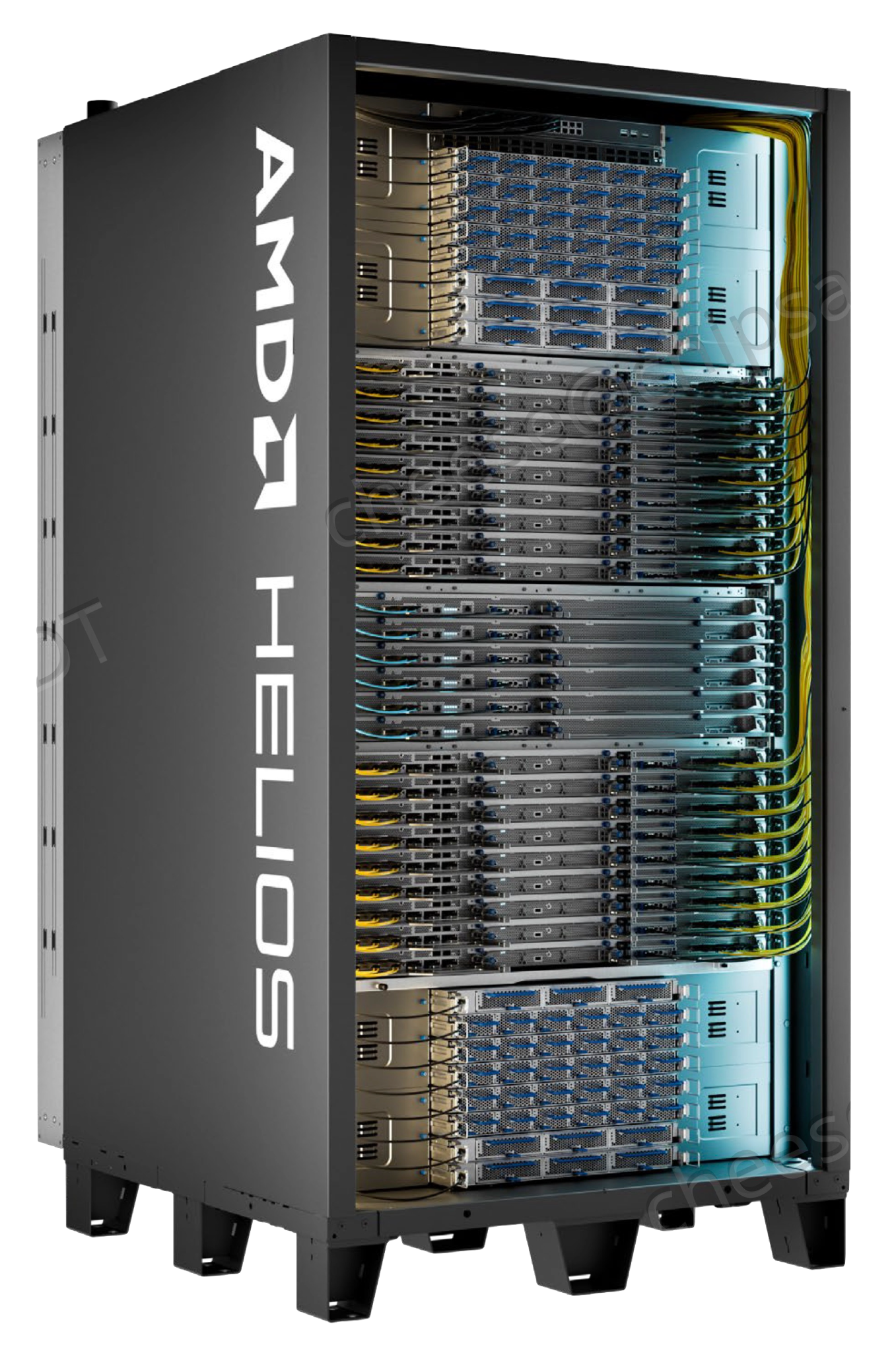
It comes along with the new Helios rackscale solution, enabling scaling to 72 GPUs in a single pod, up from 8 GPUs for previous MI355X systems. It also features a new fault-tolerant scale-up networking architecture based on UALink over Ethernet (UALoE) with single-hop all-to-all communication across the entire rack.
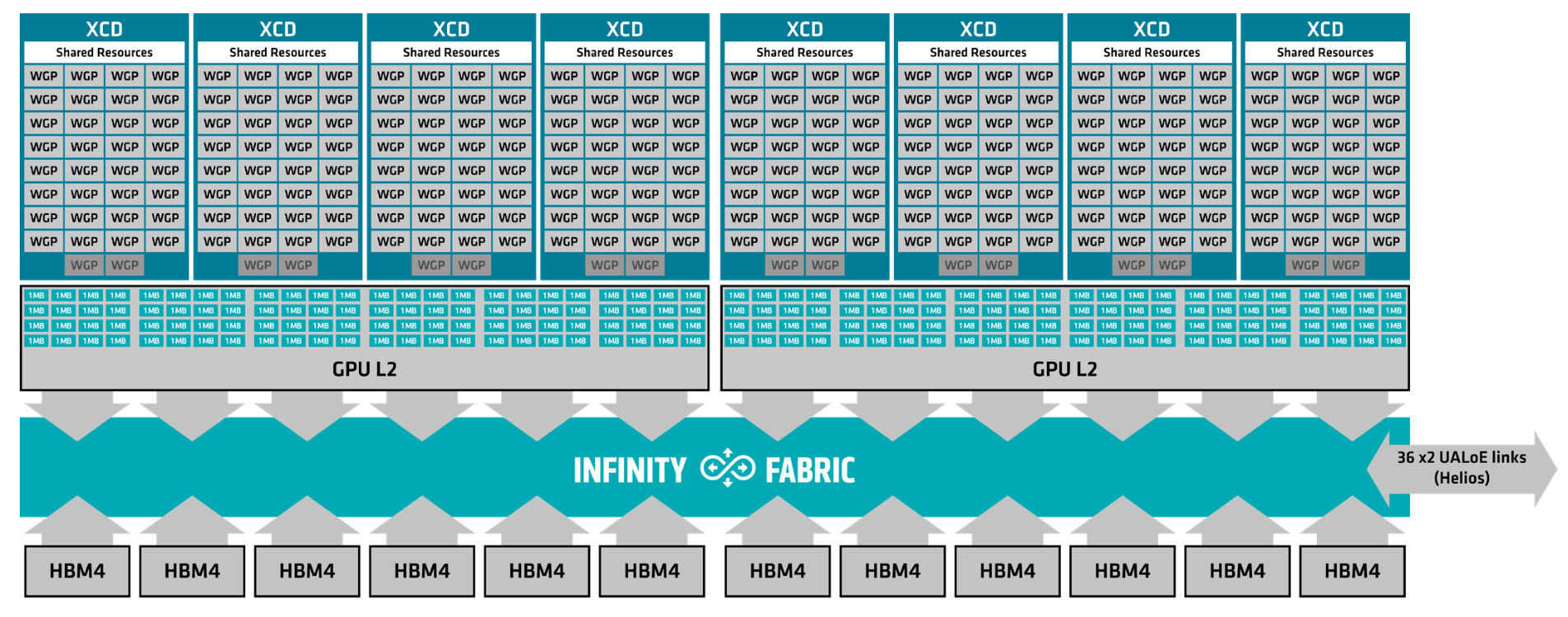
A single MI455X contains 256 Work Group Processors (WGPs) across 8 Accelerator Complex Dies (XCDs), with a max “engine” clock of 2.4GHz. This enables peak compute figures ranging from 315 TFLOP for matrix/vector FP32 and vector FP16, and up to 40.26 PFLOP for OCP MXFP4. This is paired with 12 stacks of HBM4 each on a 2048 bit bus for a total of 192 channels, giving each GPU a total of 432 GB of memory at 23.3 TB/sec.
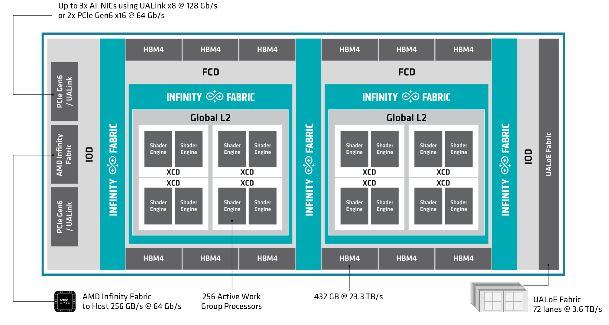
Starting with the changes in the “Compute Unit”, AMD now counts the WGPs instead of the CUs for CDNA5. Unlike what they have done on their consumer counterparts where each WGP counts as two CUs.
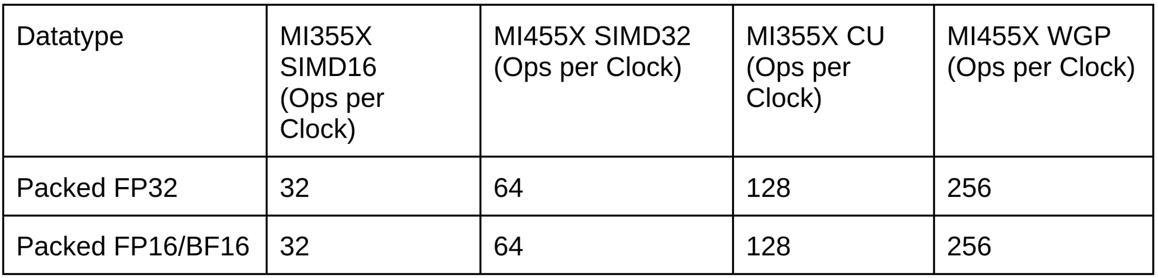
But just like RDNA4, each WGP comprises four dual issue Wave32 SIMD32 units alongside 4 scalar units which is a massive change from CDNA4’s four single issue Wave64 SIMD16 units.
This means that each WGP can do up to 256 packed FP32 operations per cycle (512 FLOPS if using FMA).
To support this new SIMD design, the VGPR register file has been reorganized with any wave now able to address up to 1,024 VGPRs which is four times the number of VGPRs that a wave could access in prior CDNA and RDNA architectures. Each SIMD still has 128kB of vector registers just like CDNA4 which means it has twice as many (1024) registers available in practice due to Wave32 vs Wave64, but it is still less than the 192kB available on RDNA4. It also means that a single wavefront is in some cases expected to occupy the entire SIMD.
The matrix units also have been beefed up with each matrix unit being able to do up to 8,192 FP4 operations per cycle and with 4 matrix units per WGP you can do up to 65,536 matrix operations per cycle per WGP.
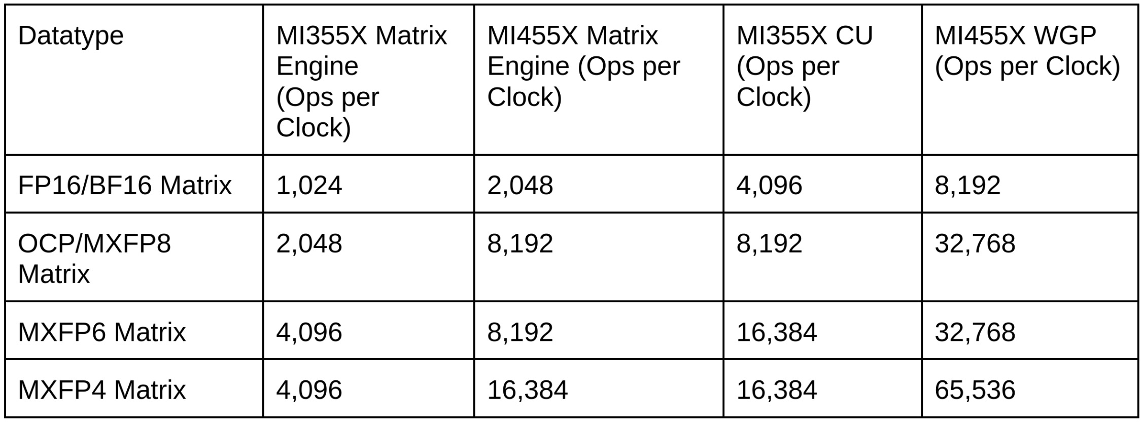
This means that only FP4 and FP8 are practically faster in the new architecture, and the rest of the performance comes from increasing the SIMD width from 16 to 32.
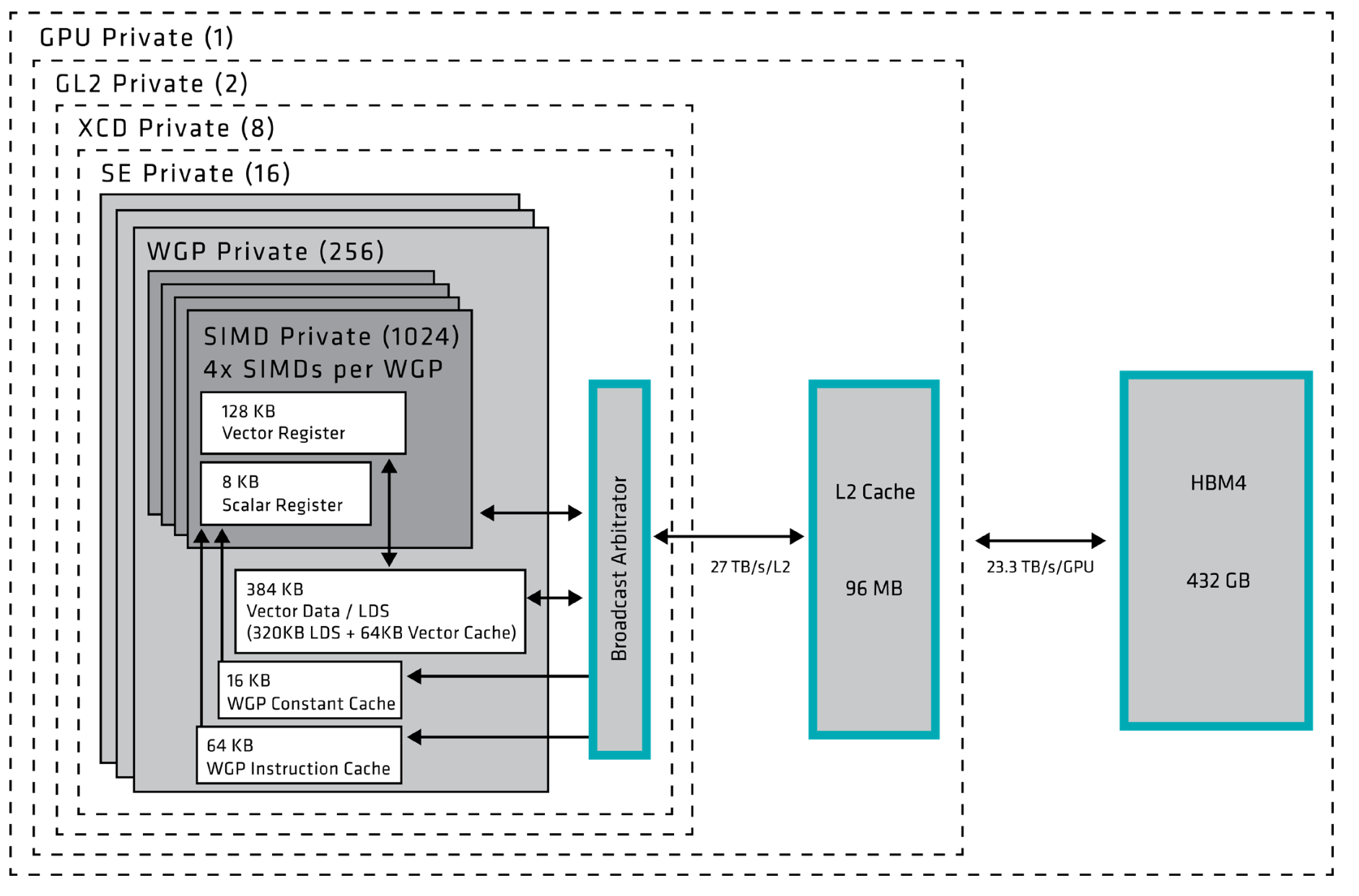
The inter-WGP caches have also changed to support this new design. Both the L1 Data Cache and the LDS have doubled in size to 64 KB of L1 Data Cache and 320 KB. The bandwidth of these caches has also doubled and can now do 2 256 bytes per clock.
Each XCD has 32 WGPs active, 34 physical WGPs of which 2 are fused off, which are broken up into 2 Shader Engines (SE) per XCD each with 16 WGPs. A shader engine is paired with a “Broadcast Arbitrator” replacing the L1 buffer (GL1) from RDNA4, which is now at the SE-level instead of the lower shader array-level. It works both as a write-combine buffer along with providing “up to 4x” bandwidth amplification by presumably broadcasting data.
The memory subsystem now allows multicast loads, accelerating matrix multiplication significantly by reducing redundant memory traffic. Imagine a GEMM that calculates C=A×B, then normally we would have each wavefront individually load a tile of, for example the A operand into the LDS of each WGP. With multicast loads we can instead load this tile of A into all relevant WGPs with a single multicast load instruction.
Each wavefront still loads a different B tile, but MI455X can fetch the common A data from L2 once and use the Broadcast Arbitrator to replicate it into all relevant WGPs private LDS allocations.
AMD calls this up to 4x bandwidth amplification, though the amplification happens after L2 and it does not quadruple L2 or HBM bandwidth. Instead, one unit of L2 traffic becomes four units of locally delivered data, reducing redundant cache reads and chiplet-link traffic while leaving each WGP with a nearby copy of the data.
Moving down to the base dies, MI455X has 192 MB of Global L2 cache split across two Fabric Cache Dies (FCDs). Each FCD contains 96 1 MB SRAM blocks, giving it 96 MB of L2 capacity for the 128 WGPs attached to that cache domain. Each FCD can deliver up to 27 TB/s of L2 bandwidth, for an aggregate of 54 TB/s across the package.
This arrangement also changes how the cache domains behave. On CDNA 3 and CDNA 4, CUs attached to one base die could access the cache on another base die within the same package. CDNA 5 removes that capability: a WGP attached to one FCD cannot access the L2 cache on the other FCD. In that respect, MI455X behaves more like an AMD EPYC CPU, where a core on one CCD cannot directly access the cache attached to another CCD.
AMD made this change to improve the behavior of atomic operations across XCDs, eliminate the kernel flush boundary that MI300-series XCDs required for global visibility, and increase L2 data reuse. Although the two L2 domains are isolated from each other, each 96 MB cache can hold data associated with any global address in the GPU. That allows a WGP’s local L2 domain to cache data that might otherwise require traffic across the die-to-die interface.
Speaking of that interface, the two FCDs are connected by a die-to-die interconnect providing approximately 14 TB/s of bidirectional bandwidth. The FCDs are also connected to 12 stacks of HBM4, with each stack providing 36 GB of capacity over a 2,048-bit interface. At approximately 7.6 GT/s per pin, those stacks provide a combined 432 GB of HBM4 and 23.3 TB/s of memory bandwidth.
For any I/O that is external to a MI455X package, each FCD is attached to a IO die which does the very important job of connecting the GPU package to the host CPU, the scale-up network, and to the scale-out NICs. The CPU to GPU link that was previously serviced by PCIe has been replaced by a dedicated 16 lane AMD Infinity Fabric providing 256GB/s of bi-directional bandwidth which allows a coherent link between the GPU package and the host CPU.
Speaking of scaling up, along with the MI455X accelerator AMD is launching a validated rackscale platform for large scale AI infrastructure deployment. This is enabled by an increase in scale-up interfaces with MI455X having 36 x 400Gbit/s UALoE interfaces that implement 2 x 200G ethernet lanes each, comprising 3.6 TB/s of peak bidirectional bandwidth per GPU.
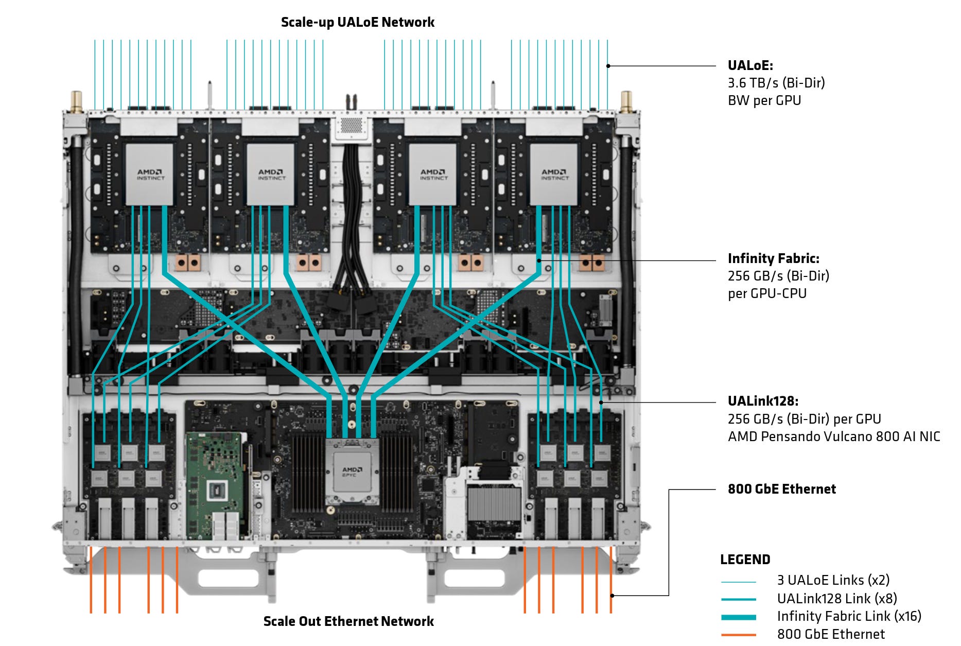
MI455X also introduces a split DMA architecture, which automatically associates traffic with the optimal link that reduces the topology awareness required for communication.
Helios uses OCP’s new Open Rack Wide form factor, compromising a cabinet 1.2m wide and 1.3m deep that provides. GPU’s are arranged in two groups of nine Compute Trays, each 1 OU in height. Each tray has four MI455X’s and one 96 core EPYC 9006 SP7. Each CPU is paired with 16 x 64GB DIMMS (for a total of 1TB of memory) and five E1.S slots for SSD’s. Six Helios Switch Trays provide a total of 12 switches connected directly via 3 UALoE links per GPU. Each switch provides 432 links at 200Gb/s, for an aggregate of 21.6TB/s per switch. This amounts to a scale-up bandwidth of 260TB/s bidirectionally.
Scale-out is provided via two boards that can contain either 4 or 6 Pensando NICs, depending on how much scale-out the end customer would like, providing up to 43TB/s of backend bandwidth. With 72 GPUs in one rack, a Helios deployment is able to provide up to 2.9 EF at MXFP4 or 22.6 PF at FP32, alongside 31TB of shared HBM4 at a combined 1.7PB/s of memory bandwidth.
The basic GCN microarchitecture underpinned every single one of AMD’s compute accelerators for nearly 15 years starting with Tahiti, followed by Fiji, Vega, and the first 4 generations of CDNA. With CDNA5 AMD has moved over to a microarchitecture that is based on the RDNA series putting a bookend to the long-lived line that was the GCN microarchitecture.
And with that bookend comes the start of a new story for AMD’s Datacenter Accelerators, one that now isn’t just about a single GPU but scaling to 72 GPUs in a rack along with scaling the number of racks. For that AMD is relying on nearly every part of their business from EPYC Server CPUs, to Pensando Networking, to the base GFX12 from the Radeon Division, to combine all of them into the AMD Helios Rack.
2026-07-20 17:23:59
Hello you fine Internet folks, this article is a sequel to the Scrying the AMD GFX1250 LLVM Tea Leaves article where we are going to look at the differences between GFX1250 and GFX1251.
So if you want to know what GFX1250 is changing compared to the prior generation of CDNA along with RDNA4, I would recommend reading that article first then coming back to this article.
Starting with what is shared between both GFX1250 and GFX1251, they both inherit LLVM’s common GFX12.5 target which includes Wave32-only execution, 64-bit literals, a 32-bank LDS, packed FP32 operations, FP8 conversion support, and 1,024 addressable VGPR. Both targets also have 320 KiB of addressable LDS along with the same GFX12.5 SWMMAC instruction sets and the same WMMA and transcendental co-execution hazards.
The scheduling model is similarly close as well, with the notable exceptions being 64-bit math and WMMA AKA matrix math. Outside of those two cases, LLVM shows both GFX1250 and GFX1251 as having the same latency for 32-bit, LDS, and scalar memory operations along with the same modeled branch and VMEM costs among other similarities.
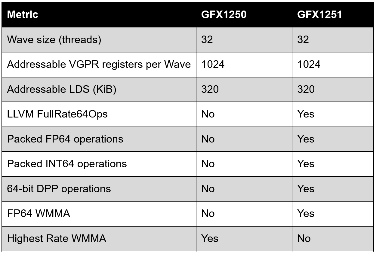
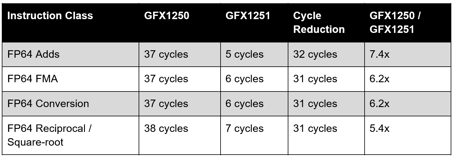
The biggest difference between GFX1250 and GFX1251 is the 64-bit paths on GFX1251 getting a significant improvement. LLVM gives GFX1251 the same ‘FullRate64Ops’ feature as prior CDNA-based accelerators which means that the compiler expects the hardware to have full-rate operations for most FP64 instructions.
Moving to packed arithmetic, GFX1251 adds v_pk_add_f64, v_pk_mul_f64, v_pk_fma_f64, v_pk_min_num_f64, and v_pk_max_num_f64 where each instruction operates on a v2f64 or two 64-bit values per active SIMD lane. Because a VGPR contains 32 bits per lane, every packed FP64 operand occupies four VGPRs meaning that the three sources consume 12 VGPRs and the result consumes four.
v_pk_fma_f64 v[4:7], v[8:11], v[12:15], v[16:19]Across a Wave32, one instruction represents 64 FP64 FMAs operations which equates to 128 FP64 FLOPS.
The packed integer side follows the same 128-bit register layout. GFX1251 adds v_pk_add_nc_u64, v_pk_sub_nc_u64, and v_pk_lshl_add_u64, each operating on two unsigned 64-bit values per lane. Those instructions are useful for paired address calculations and counters, though LLVM does not expose a packed U64 instruction set as broad as the FP64 one.
Importantly, LLVM’s optimizer does know these instructions exist because the GFX1251 cost model advertises a 128-bit fixed vector width when packed FP64 or U64 operations are available, permits a vectorization factor of two for 64-bit elements, and cuts the estimated cost of work in half. In other words, this is not just an ISA feature for hand-written assembly, LLVM is being taught to combine pairs of 64-bit operations so that regular compiled code can use it.
The v_wmma_f64_16x16x4_f64 instruction for FP64 Matrix Math is a GFX1251-only instruction appropriately enough in the LLVM feature set labeled GFX1251GEMMInsts. Notably, despite the feature set implying multiple instructions in this set, as of the time of writing the only instruction in this feature set is v_wmma_f64_16x16x4_f64.
v_wmma_f64_16x16x4_f64 v[8:23], v[0:3], v[4:7], v[8:23]Per wave, the two matrix inputs consume four VGPRs each, while the accumulator and result occupy 16 VGPRs. Across a wave, the instruction updates a 16x16 FP64 output tile over a K dimension of four. That works out to 1,024 FP64 FMA operations or 2,048 FLOPS per wave with LLVM scheduling it as a four-pass WMMA instruction with a 16-cycle latency.
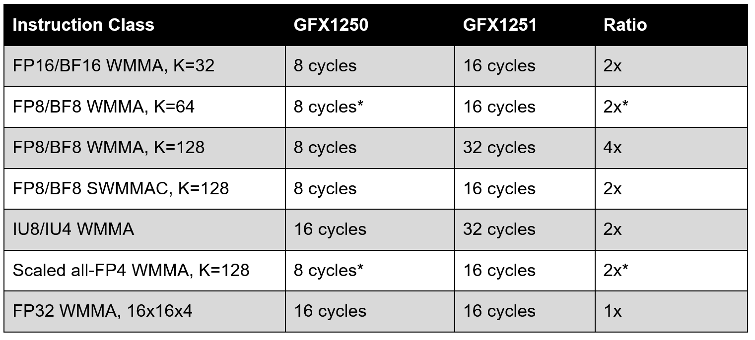
The tradeoff for all of this FP64 compute is a reduction of low precision matrix math. LLVM enables GFX125xLowestRateWMMA for GFX1251 and places many instructions into latency classes that are two to four times as long as GFX1250’s.
The slower instruction rate also makes GFX1251’s dependency hazards longer. LLVM groups GFX12.5 WMMA instructions into rate categories and counts the number of unrelated VALU instructions or `v_nop` slots required between dependent operations. The slowest GFX1251 category can require up to 17 intervening slots before a dependent WMMA operation and 16 before a dependent VALU operation, whereas the faster categories require only 9 slots before a dependent WMMA operation and 8 slots before a dependent VALU operation.
GFX1250 and GFX1251 share enough features that calling them members of the same GFX12.5 family makes sense. They use the same wave size, expose the same architectural VGPR range and LDS capacity, and look almost identical to LLVM for ordinary 32-bit and memory operations which points to GFX1250 and GFX1251 using the same base architecture.
However, it is very clear that AMD has decided to specialize the two GFX12.5 architectures far more than even the MI300 family. The MI300 series had the MI300A and MI300X which while specializing the SoCs, with MI300A having 3 Zen 4 CCDs plus 6 CDNA3 XCDs onboard compared to MI300X having 8 CDNA3 XCDs, reused the same XCDs between them. The MI430X and MI455X are very clearly not sharing the same XCDs but have specialized the XCDs for either HPC or ML workloads.
GFX1250 is the better target for low-precision matrix math. Depending on the instruction, GFX1251 takes two to four times as many modeled cycles and can require much longer spacing before dependent operations. GFX1251 instead gets full-rate FP64, packed FP64 and U64 arithmetic, 64-bit DPP, and support for FP64 matrix math.
That makes GFX1251 much more interesting in the broader HPC space. A large portion of traditional HPC still depends on FP64 for numerical stability and reproducibility, including computational fluid dynamics, weather and climate modeling, molecular dynamics, finite-element analysis, seismic processing, quantum chemistry, and other scientific workloads. These applications do not only need a high peak FP64 number, they also need FP64 arithmetic, conversions, reductions, address calculations, and dense linear algebra to work well together. GFX1251’s full-rate FP64 path, packed 64-bit instructions, 64-bit DPP support, and FP64 WMMA instruction all point to a HPC focus.
FP64 matrix operations are especially relevant because DGEMM sits underneath a large amount of scientific computing, directly through BLAS and LAPACK or indirectly through larger simulation and solver stacks. A 16x16x4 FP64 tile does not by itself establish application performance, but it gives GFX1251 a dedicated way to accelerate the double-precision matrix math used by workloads such as HPL and dense numerical solvers. Meanwhile, packed FP64 and 64-bit DPP should help with the less tidy vector math and reductions which make up a good portion of HPC compute. That makes the overall FP64 story both broader and stronger than adding one impressive matrix opcode.
In the end what we are seeing with the GFX12.5 family is a story of different architectures for different markets. While GFX1250 is very much focused on the insanely lucrative ML market, GFX1251 is focused on the still very important HPC market where high precision compute still reigns supreme.
2026-07-19 11:21:03
In just a few short days, AMD will be showing off their brand new MI400 series of Datacenter Accelerators at their Advancing AI event but before that event comes, we thought it would be fun to attempt to scry the tea leaves that are LLVM commits to see what we can ascertain about this next generation of AMD accelerator.
LLVM currently has preliminary support for two new accelerators from AMD, under the codenames GFX1250 and GFX1251.
GFX1250 is an accelerator chip oriented at the machine learning market called MI455X and will be what powers the Helios rack. While the GFX1251 is oriented at the HPC market, named the MI430X and is projected by AMD to deliver over 200 TFLOPs of native double-precision compute.
We’ll focus on the GFX1250 for now though and save the GFX1251 for another day.
We’ll compare the architecture to the consumer variant, the previous generation of CDNA accelerators, and to some extent Nvidia’s Blackwell.
A curious note here is that while we know that these accelerators are not APUs, they are listed as such in LLVM.
The biggest similarity with the consumer architectures is that we now have a WGP (Workgroup Processor) that are built up from two pairs of two SIMD32 arrays, but there is also four SIMDs per CU just like there was in GCN and CDNA. This seeming discrepancy is because there is no longer any need for the software to separate the two CUs in the WGP and AMD seems to use the terms interchangeably.
This “change” is probably not as structural as it might at first seem and might not even exist in hardware, the changes in the caching hierarchy simply makes the distinction pointless for the compiler as there is now a shared vector L0 cache for the whole WGP.
GFX1250 operates only in Wave32 mode, unlike RDNA that can run in Wave64 in addition to Wave32 mode. Prior CDNA GPUs can only run in Wave64 mode and we can expect to see some oddness there from a performance engineering point of view when porting things to the new accelerators and a lot of kernels will have to be re-evaluated for the new architecture.
It also seems like GFX1250 can run 20 waves per SIMD, which is four more than RDNA4 can do.
We do not know if any of these characteristics are a sign for where AMD goes on their GPUs, but I personally guess that it is a sign of times to come and a future generation of AMD GPUs will be locked to Wave32 and the “WGP” as it currently exist goes the way of the dodo but it seems like this is not happening anytime soon.
Similarly to RDNA4 we now get “WMMA” support, unlike the older “MFMA” featured in CDNA and this is where most of the machine learning capabilities of the GFX1250 will come from and we’ll look into it more later.
The dynamic VGPR allocation feature that was heavily touted in RDNA4 is missing, which is a bit strange to me since I would imagine it is even more important for machine learning workloads that are under much higher register pressure due to working with whole tensors instead of just individual vectors or matrices. The mode-switch is still there but the instruction to allocate new registers is documented as a no-op.
One of the largest changes found in GFX125X is that each wave in a SIMD can now address up to 1024 Vector General Purpose Registers (VGPRs) from the Register File. This is a major improvement over prior CDNA generations where you had a split allocation of registers with up to 256 VGPRs and 256 Accumulation VGPRs, which can only be used by the matrix units, for a total of up to 512 registers allocated to a single wave at a time.
This is an even larger improvement over the register allocation behavior of the RDNA series of GPUs, RDNA can only allocate up to 256 registers to a single Wave with no allocation split. This is a major update that might at some point be part of a future generation GPU IP but I wouldn’t bet on it coming soon. We will just have to wait to see if the feature is going to stay locked to the Instinct line or if this ability to allocate up to 1024 registers to a single wave will make an appearance in the Radeon line up as well.
The maximum addressable local memory (LDS) is now 320kB per wavefront which is twice as much as CDNA4 and dwarfs the 64kB addressable in RDNA. But the actual LDS can actually be even larger, a major change in GFX125X is the merging of the LDS and vector L0 caches into what AMD is calling the WGP Cache (WGP$). While both Nvidia and Intel have had a single structure for both cache and shared memory for a long time, AMD has been the odd vendor out with a split cache and LDS. GFX1250 now has a single 448KB structure that can be broken up into different allocations depending on what the compiler or programmer requests.
GFX1250 still supports packed fp32 operations allowing a single lane in the SIMD to process two fp32 operations at once just like CDNA2 and later, this practically means that when using packed instructions it has twice the vector width of RDNA.
It also inherits the more numerous and powerful SDMA units from CDNA.
It is notable that Nvidia and Intel do have some vestigial graphics hardware left on their accelerators and GFX125x differs a little from their offerings on this front.
No export instructions and therefore no rasterizer (like CDNA)
No image (texture) instructions (like CDNA)
No BVH (raytracing) instructions (like CDNA)
No vector parameter interpolation instructions that are used to access and interpolate vertex data in pixel shaders (like CDNA)
No MTBUF (typed buffer) instructions are supported (unlike CDNA and RDNA3)
No MUBUF (untyped buffer) instructions are supported (unlike CDNA and RDNA)
No LDS parameter and parameter direct loads (like CDNA)
We’re seeing that this GFX125x is even more of a pure compute accelerator than even prior CDNA architectures with nearly all graphics features having been removed. This probably saves a little bit of die space and removes features no one will miss, so it makes a lot of sense to me.
The headline feature of the MI455X is its AI capabilities, and the tensor units are what powers that. This seems to be a best of both worlds situation where AMD is combining the simpler programming model from RDNA4 with the higher performance and capabilities of CDNA4.
On RDNA4 WMMA operations are M = N = K = 16 (matrices are 16x16) except for the 4-bit ones that have K = 32 (arguments are 16x32 or 32x16 and accumulated into 16x16).
GFX1250 keeps M = N = 16, but K instead is the same as it was on CDNA4. K = 4 for 64-bit and 32-bit floating-point elements, K = 32 for floating-point 16-bit elements, K = 64 for fixed-point 8-bit elements and K = 128 for floating-point 8-bit elements. Interestingly the i4 operations stay at RDNA4 level at K=32 and are no longer a very popular data format in large AI inference scenarios due to the adoption of MX floating point operations.
Unlike on RDNA4 the sparse versions of WMMA seem to do less work per instruction than the dense ones by keeping K the same.
RDNA4 supports the following matrix of formats for WMMA
While CDNA4 supports the following for MFMA
And GFX1250 seems to support all the datatypes that are found on both CDNA4 and RDNA4 except for fp64 which seems to be restricted to GFX1251, including the support of OCP MX-style scaling that was previously available solely on CDNA4.
In addition there’s new instructions that allow you to transpose submatrices in LDS to complement the ones already in RNDA4. The fp4/fp6 versions of these have their own feature flag, that might be a sign that these will show up on consumer GPUs or it is just a coincidence.
This seems to be AMD’s version of “Thread Block Clusters” that Nvidia introduced in their Hopper architecture, and it seems like they allow you to schedule a cluster to a specific shader engine and seems to be a feature that will be available on future graphics hardware too.
In addition to allowing you to access the cluster information, AMD has also introduced cluster-level loads which allow you to write to the LDS of other workgroups within a cluster, similar or equivalent to multicast loads on Nvidia hardware.
Author’s Note: A claim that wasn’t substantiated about DSMEM was removed here.
GFX1250 adds support for cluster-level barriers, which is a feature that is essentially required to make use of clusters and is equivalent to the Nvidia feature of the same name.
In addition we’re getting intrinsics for barrier arrival, the equivalent of mbarrier.arrive in Nvidia PTX. AMD does seem to take this support one step further though by not just implementing barriers in hardware but also full monitors, allowing the wave to be notified if a specific cache line is modified or evicted from the L2 cache.
It’s unclear what these exactly are intended to be useful for since Nvidia doesn’t have a direct equivalent already, but I guess GPU programmers will find a lot of good uses for these intrinsics.
In addition to the split barriers and barrier objects already added in RDNA4, it also supports 16 named barrier objects. These are likely added as a compatibility thing, since they have been around since Nvidia’s Tesla architecture from 2006.
AMD is adding hardware support for tanh, which is rare in traditional geometry but very common in neural networks as an activation function and in the solution of many differential equations.
But the whole unit seems to have been improved, they added bf16 support and the latency for fp32 operations have gone down from 9 cycles in RDNA4 to 8 cycles in GFX1250.
With GFX1250 we now have intrinsics to do 32x4B, 16x8B, and 8x16B atomic loads and store to global memory, the funky naming is because these are actually 128B atomic loads and stores, the first number implies how many lanes of each wavefront are involved in the atomic but the result is essentially 1, 2, or 4 complete 128B atomic memory operations.
At the hardware-level they aren’t special instructions but just a sequence of regular loads or stores that the hardware knows how to handle so that they end up on the bus correctly.
The first use-case for this that will pop into certain peoples minds is to use this to accelerate RPCS3’s Cell emulation, and while someone is obviously going to try and use it for that, there’s a bunch of use-cases for this. But a goal is likely to accelerate AMD’s equivalent to Nvidia’s Collective Communications Library (NCCL), creatively named ROCm Collective Communications Library, as explored in the paper Demystifying NCCL.
LL128 support was to some extent already enabled on CDNA but the format has now been changed to be equivalent to the Nvidia one instead of splitting into two 64B halves.
For technical reasons these operations are not available over PCIe but I assume these will be usable over CXL and UALink. Nvidia has a very similar limitation that it is only available in global memory or over NVLink.
Nvidia’s marketing name for this feature is the “Tensor Memory Accelerator”, and while this feature was already available to some extent in earlier CDNA iterations it has now gained more features especially related to tensors.
The basic version just allows you to load data from global memory into LDS without using the VGPRS.
While it isn’t completely clear to me exactly what capabilities are available to the tensor version since the types involved are opaque, the code isn’t totally obvious and the documentation isn’t completely clear. But Triton has some good documentation where the capabilities are enumerated. It is somewhat similar to Nvidia’s tcgen05.cp in capability except they transfer between global memory and LDS instead of between shared memory and tensor memory.
GFX1250 adds explicit prefetching of vector memory, and AMD has finally added this feature that is available on many CPUs that are old enough to vote. Nvidia has supported this since Fermi so it really isn’t that exciting.
Some people might think that this has been a curious omission for GPUs, but unlike CPUs we’re rarely starved for registers so we can load data early and we can use the many waves running on the same core to hide the latency.
But I can imagine that inference kernels can gain some minor performance from this so it makes sense to add now I guess.
On AMD GPUs and accelerators the hardware can most of the time figure out data dependencies automatically, but in certain cases you need to do it manually.
On GCN and by extension CDNA you had three counters that allowed you to wait on operations to be completed so that you could ensure that previous operations had been completed before continuing.
VM_CNT for vector memory operations.
Incremented when a vector-memory load is issued and decremented when the data is written to the VGPRs.
Incremented when a vector memory store is issued and decremented when the data is written to L2 cache.
Incremented when a sample or image instruction is issued and decremented when the data is returned to VGPRs.
LGKM_CNT for LDS, GDS, Konstant (scalar memory read), and Message instructions.
Incremented when a LDS or GDS load is issued and decremented when the data is written to the VGPRs.
Incremented when a LDS or GDS store is issued and decremented when the data is written to the LDS or GDS.
Incremented for every DWORD worth of scalar load issued and decremented again for every DWORD read from the scalar data cache (SMEM)
Incremented for every message send issued and decremented when the message is actually sent.
EXP_CNT for VGPR exports, this is a graphics feature used for passing things like vertex positions and color values between shaders. This exists in CDNA but isn’t used so we’re going to conveniently ignore this counter
The big issue here with the GCN/CDNA setup of these counters is that instructions of different types are returned out-of-order. And in the case of scalar loads they are also returned out-of-order even within the same instruction type.
This regretfully means that you are likely to need to insert more waits more than would otherwise be required, especially for scalar reads where waiting for the counter to reach zero is the only useful value.
So AMD redesigned this part of the instruction set for RDNA4 and made it much more fine-grained. We now have a lot more of these counters.
LOADcnt counts the number of vector loads issued but not yet completed, similar to the first part of VM_CNT.
STOREcnt counts the number of vector stores issued but not yet completed, similar to the second part of VM_CNT.
SAMPLEcnt counts vector sample/gather/msaa/lod instructions issued but not yet completed, similar to the third part of VM_CNT.
DScnt counts the number of LDS instructions issued but not yet completed, equivalent to the first half of LGKM_CNT.
KMcnt counts the number of scalar loads and message sends issued but not yet completed, similar to the second half of LGKM_CNT.
EXPcnt counts the number of export or parameter loads outstanding, similar to EXP_CNT.
BVHcnt counts the number of vector memory BVH (raytracing) instructions issued but haven’t returned data yet. There’s obviously no GCN or CDNA equivalent since there’s raytracing hardware.
This means that RDNA4 has a lot more situations where it can avoid having to explicitly stall the core even though there is useful work to perform compared to GCN or CDNA prior to GFX1250.
And while this isn’t as big of a deal in compute tasks, in modern graphics tasks it does make a difference since for example you can issue texture reads far ahead and not have that block a regular memory load.
On GFX125x we don’t have the following graphics wait counts,
SAMPLEcnt doesn’t exist because there are no texture samplers.
EXPcnt doesn’t exist because there is no rasterizer.
BVHcnt doesn’t exist because there are no raytracing instructions.
But to compensate we get new ones that do not exist in RDNA4 at all,
ASYNCcnt, counts the number of outstanding asynchronous load and store instructions to LDS.
TENSORcnt, counts the number of outstanding tensor load and store instructions.
Xcnt, counts the number of memory operations that have not completed address translation yet and a wait here is required to be inserted before instructions that must not be retried in case of a page fault or similar.
The final one is either the most or the least interesting one to you, since it allows a simpler way to guarantee atomicity during XNACK replay.
It seems like a good improvement and AMD is catching up on features with both Hopper and Blackwell, hopefully that means that they can not only beat Nvidia in theoretical performance but also challenge the market leader in practical performance with MI455X and Helios.
2026-07-14 09:23:37
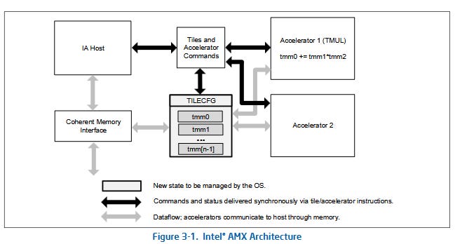
CPU designs must evolve to keep up with changing workloads. Sometimes, that evolution involves extending the instruction set to efficiently represent certain types of work. Intel’s AMX extension is one such example. AMX accelerates matrix multiplication for machine learning workloads by providing a set of 2D tile registers and configuration registers. Programmers can then configure specialized execution units (“accelerators”) to target matrix data in those tile registers. AMX was first implemented on Intel’s Sapphire Rapids server CPUs with a tile matrix multiply unit (TMUL) accelerator. Now, the x86 Ecosystem Advisory Group has written up a whitepaper and specification for ACE, which introduces a second accelerator type. While ACE is an AMX accelerator alongside TMUL, I’m going to call them “AMX” and “ACE” because TMUL was the only accelerator implementation that existed at AMX’s launch, and is still the only AMX accelerator available in hardware today. Documentation also tends to call them “AMX” and “ACE”.
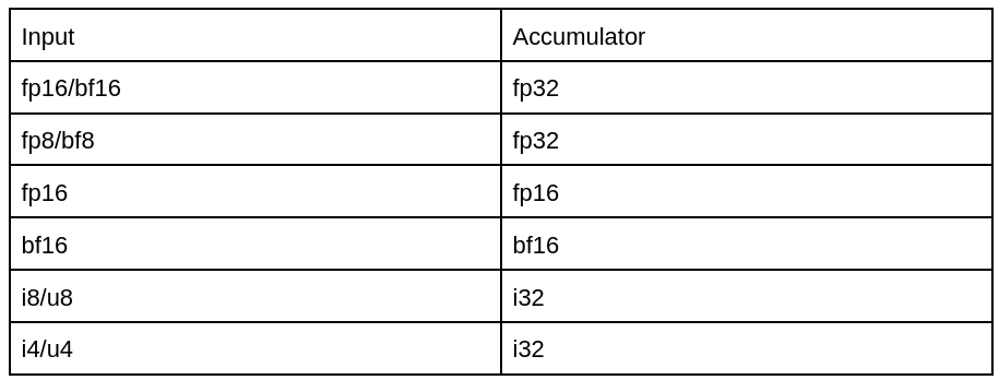
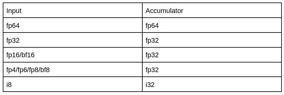
AMX TMUL offered a highly configurable setup where code would specify matrix tile parameters for each tile register. For instance, the tile register tmm0 could be set up as a 16x64 matrix of INT8 values by specifying 16 rows and 64 bytes per row (“colsb”). TMUL matrix multiply instructions like TDPBSSD would take the tile configuration into account and perform an entire matrix multiplication operation between specified tiles. On the data type side, AMX TMUL could operate on INT8, FP16, and BF16 values. The latest iteration of TMUL, implemented on Granite Rapids-D CPUs, also supports complex numbers with FP16 real and FP16 imaginary components.
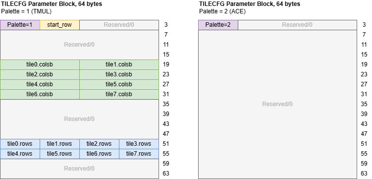
ACE does away tile register configuration options, and always considers them 64 bytes by 16 rows. Complex numbers are gone, but FP8 is in. On the compute-side, ACE provides outer product instructions instead of the inner product instructions given by AMX.
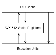
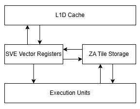
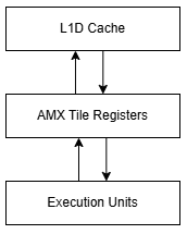
Arm’s Scalable Matrix Extension (SME) and its SME2 extension is an obvious comparison point. Both ISA extensions seek to accelerate matrix multiplication within the framework of a CPU ISA, providing a low latency alternative to using less integrated accelerators like GPUs. The two ISA extensions however differ in a number of areas. ACE is built on AMX, and continues to use AMX’s 8 KB of tile registers for holding matrix values.
Arm’s SME in contrast has a variable “streaming” vector length (SVL) just like SVE’s vector length (VL). The SVE and SME vector lengths do not need to be the same, and often are not. Like SVE, SME allows the vector lengths from 128 to 2048 bits, growing in powers of two.
The streaming vector length defines the size of the “ZA” storage array, which is SME’s equivalent of AMX tile registers. ZA storage is a 2D array where each side matches the SME streaming vector length. ZA storage capacity therefore ranges from 256 bytes with a 128-bit streaming vector length, to 64 KB with the maximum 2048-bit vector length.
While AVX512-VNNI and AMX accelerate inner products, ACE and SME accelerate outer products.
An inner product (or dot product in this special case) of two vectors a
and b is,
Or if you are a physicist you might have learned it via the geometrical interpretation of,
Where θ is the angle between the vectors. The outer product (or tensor product in the general case) of the vectors a and b on the other hand results in a rank-1 matrix C like the following.
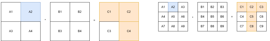
The columns of C are all proportional to a and this is how we know that it is a rank-1 matrix, but also that matrix multiplication is just a sum of outer products like,
In fact many operations in linear algebra can be seen as a linear combination of outer products, making outer products a natural primitive to implement in a processor, the most obvious example the singular value decomposition of a matrix,
isn't trivial to understand when written as an inner product, but it is just the sum of the outer product of the columns of U and V multiplied by each corresponding singular value or,
Even algorithms that aren’t as obviously converted to outer product forms like the FFT have been reformulated in terms of it to utilise SME as an accelerator. Arm gave the following example on how to do it, but if you search for papers you can find various more effective ways to do it.
We have historically mostly used inner products because that reduces the amount of state we need to keep in registers, and since that is a precious resource that has been important to optimise for.
However, as we’ve seen above almost all linear algebra can be seen through both lenses, and code can easily convert between inner and outer products. SME takes advantage of this to do matrix multiplication via outer products and ACE seeks to do the same.
Model weights are often quantized to very small bit-widths to reduce memory bandwidth and capacity pressure. ACE and SME, unlike for example NVIDIA’s TensorCores, pre-process the input vectors in software without having to bounce them via the register file.
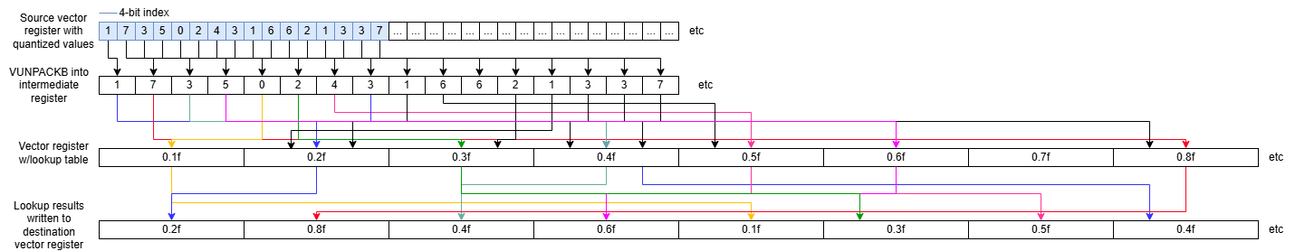
Quantized weights are converted to natively supported data types to make use of the accelerators. ACE leans on AVX-512/AVX10’s fixed 512-bit vector width to accelerate this conversion process. A 512-bit vector is large enough to hold a lookup table mapping a data type up to 6 bits to an 8-bit output using VPERMB, and for a 7-bit input VPERMI2B can use two 512-bit vector registers together as the lookup table.
A new VUNPACKB instruction added in ACE/AVX10.3 can extract 2 to 7-bit elements into byte-aligned positions and then the previously mentioned vector permute instructions can perform the data type conversion. ACE thus provides a degree of future proofing by being able to handle any data type between 2 and 7 bits with just these three instructions, and you can with software implement essentially any method of your choosing.
The x86-64 EAG also hopes this flexibility will let ACE hardware apply to applications beyond de-quantizing model weights, such as codebooks for compression of data.
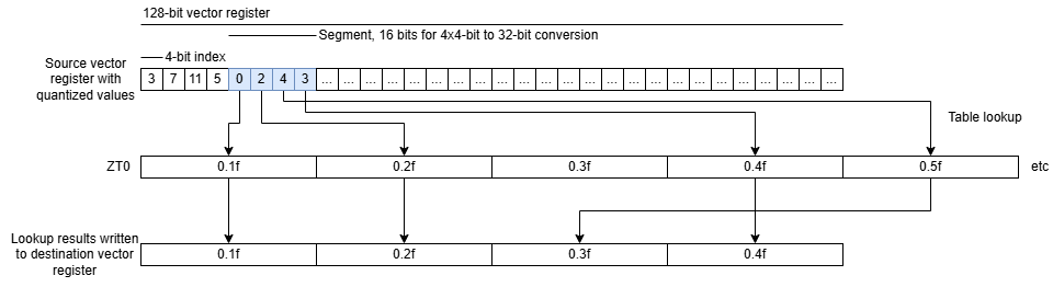
Arm can’t rely on having vector registers wide enough to work as lookup tables for data conversions, because SVE lets implementations define streaming vector lengths from 128 to 2048 bits. SME2 therefore adds a 512-bit ZT0 register specifically designed to work as a 16 x 4B lookup table. LUTI2 and LUTI4 instructions perform data conversions by decompressing 2-bit or 4-bit index values from a vector register, looking up their values in ZT0, and placing output values into a destination vector register.
Adding the fixed width ZT0 register lets Arm accelerate data conversions within the variable vector length SVE/SME framework, but isn’t as flexible as ACE’s VUNPACKB + permute combination. Model weights quantized down to anything other than 2 or 4 bits wouldn’t benefit from SME2’s lookup table acceleration and more complicated codebook approaches that require multiple different lookup tables cannot be supported.
On the other hand, SME2’s mechanism lets Arm express a data type conversion with a single instruction instead of two. It also reduces pressure on vector registers, because the lookup table is stored in a separate register and LUT instructions don’t need a separate vector register to hold intermediate unpacked values. On the flexibility front, Arm could continue extending the ISA and add LUT instruction variants to support more data type widths.
Low precision data types like FP8 suffer from low dynamic range. The Open Compute Project’s Microscaling Formats specification tackles this with scaling factors. One scaling value applies across a block of values, increasing the dynamic range of multiplication results without increasing the bit width of each data element. ACE supports this with a new 1024-bit Block Scale Register named BSR0. BSR0 is divided into two 512-bit halves, one for each of the two inputs of an outer product operation. Each half is further divided into four groups of 16 8-bit scale values, selected by an immediate operand in outer product instructions.
Arm’s SME supports scaling via 8-bit LSCALE and LSCALE2 fields in the Floating Point Mode Register (FPMR). BF1CVT uses LSCALE, and BF2CVT uses LSCALE2. Although Arm documents two instructions, the scheme is actually similar to how ACE selects BSR groups using an immediate. There’s a 1-bit opcode difference between BF1CVT and BF2CVT, which a creative decoder could treat as an immediate. Using scale factors is a two-step process with SME, where BF1CVT/BF2CVT apply a scale and a separate outer product instruction carries out the math. Update instructions for both ACE’s BSR0 and SME’s FPMR will overwrite the entire register, signaling that ISA designers on both sides don’t expect scale values to change often.
There’s a distinct possibility that neither register gets renamed in hardware implementations, so any scale value update would create a serialization barrier for FP8 instructions. If scale values do change often enough to warrant renaming, then both ISAs are in a difficult position. All of ACE’s FP8 outer product instructions reference BSR0, and therefore depend on the last BSR0 write. SME has separate instructions for scaling and outer product math, but FPMR also includes fields that control FP8 format and overflow behavior. It therefore ends up in the same situation of where all FP8 math depends on the last FPMR write.
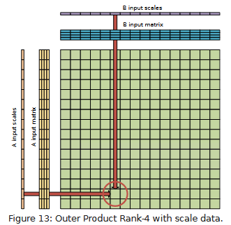
Quantization is one way to reduce memory bandwidth demands. Tiling is another. Simple matrix multiplication creates memory access patterns with poor locality. Splitting a matrix into submatrices (tiles) helps improve data reuse by fitting into high bandwidth caches, rather than frequently streaming in data from DRAM. But bandwidth challenges remain even with tiling. Even cache bandwidth can become a constraint with enough compute available. If there’s enough compute to get through tiles faster than they can be streamed in from lower levels of the memory subsystem, L2, L3, and even DRAM bandwidth can come into play.
Larger tiles help mitigate this problem. Calculating each tile of the result matrix involves multiplying each tile in the corresponding row of the first input matrix with every tile in the corresponding column of the second input matrix. Larger tiles mean a matrix can be covered with fewer total tiles. Because each input tile appears less often in an output tile’s matching row or column, it’s loaded fewer times throughout the matrix multiplication process.
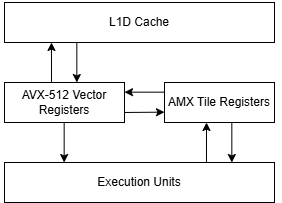
Register capacity influences tile size, because we want to keep the accumulator in registers. Each accumulation is a read-modify-write operation, which is two memory accesses. Moreover, most memory subsystems have less store than load bandwidth, reflecting typical application behavior where memory reads far outnumber writes. ACE keeps the same 8 KB of tile registers that AMX introduced, but changes the math instructions to take two inputs from AVX-512 vector registers. TMUL math instructions take all of their operands from tile registers, forcing code to use some tile register capacity to hold temporary input data.
For example, take a C = AB matrix multiplication operation with 32K by 32K matrices of 8-bit integer values (INT8). A and B will be input matrices, and C will be the result. The matrix multiplication requires 32768^3 or 35.2 trillion multiply-add (MAC) operations. C will be kept in registers in all cases, while A and B will only be given registers as necessary.
AVX-512 provides 32 512-bit vector registers. We can use about 24 of those registers to store accumulators for C, with the other eight used to store input values. AVX-512 FMA instructions can only take one input from memory, meaning the other input has to be loaded into registers before being operated on.
We need to load 16 x 32k elements from A and 24 x 32k elements from B to calculate our output tile, so we need to load 40 x 32k ≈ 1.3M elements from memory. We need to run this kernel 32k x 32k / (16 x 24) ≈ 2.7M times, for a total of about 3.4 TB of cache traffic. That works out to approximately 0.10 bytes loaded per MAC operation. A data cache capable of sustaining 128B/cycle of load bandwidth would be able to feed 1228 MAC operations per cycle, which is plenty considering each 512-bit vector contains 64 8-bit elements, and no CPU is likely to have over 19 512-bit vector pipes.
If we use the same trivial tiling with a SME implementation with a 512-bit streaming vector length, and a 4 byte accumulator, we get 4 SME ZA tiles of 16 x 16 elements each for a total of 32 x 32 elements. For each iteration we need to load 32 x 32k elements from A and B for a total of 2M elements in total. But we only need to run the kernel 32k x 32k / (32 x 32) = 1M times, for a total of 2.0TB of cache traffic. SME therefore cuts cache bandwidth demands by almost 50% compared to AVX-512-VNNI. At about 0.06 bytes loaded per MAC operation, a data cache capable of delivering 128B/cycle could feed 2088 MAC operations per cycle.
In addition, due to the outer product design we do not need any extra L1 traffic from spilling registers since we have plenty of vector registers available to us to do any pre-processing we want to do for practical applications.
Apple’s M4 is an example of a hardware implementation with a 512-bit streaming vector length. A hypothetical implementation with a larger vector length would benefit from further bandwidth savings. For example, a 1024-bit SME implementation would have a 64 x 64 element output, loading 2 x 64 x 32k elements and 0.25 million kernel invocations for a total of 1.0TB of cache traffic.
For AMX, we’ll use six tiles to store the output accumulator, and use one tile each for A and B. This should be doable according to my calculations and backed up by this paper you at most need to spill two tiles per seven you load which should fit trivially in L1 and therefore we’ll conveniently ignore the extra cache traffic.
Our six tile registers allocated mean that we have 32 x 48 element output, and we again need to load 32 x 32k elements from A and 48 x 32k elements from B per kernel invocation for a total of 2560 tile loads. But to compensate we just need to run the kernel 0.7 million times for a total of 1.7 billion tiles loaded or 1.7TB of cache traffic. That works out to 0.052 bytes loaded per MAC operation, meaning a 128B/cycle L1D could feed 2457 MACs/cycle.
If we instead used Intel’s recommended strategy we would need to run the kernel 1.0 million times and load 2048 tiles per invocation for 2.0TB of data loaded which is so significantly worse that I am going to conveniently ignore this number for the rest of the article since I can’t think of an obvious reason you would ever do this tiling strategy.
ACE matrix instructions take inputs from AVX-512/AVX10 vector registers and accumulate into tile registers, so A and B don’t have to be kept in tile registers like with AMX. That allows for a larger 32 x 64 element output. We need to load 96 x 32k elements for a total of 48k vector loads but with a mere 0.5 million kernel invocations for a total of 1.5 TB of cache traffic. At 0.046 bytes loaded per MAC operation, a 128B/cycle L1D would be able to feed 2785 MACs/cycle.
If M = N = K and Ta and Tb are the dimensions of the tile, then we need to load (Ta + Tb) x N elements per kernel invocation, and require N x N / (Ta x Tb) kernel invocations for a total of (Ta + Tb) x N x N x N / (Ta x Tb) elements loaded.
Now that I have done all the calculations I can reveal to you who glossed over the earlier numbers that the general lower bound for the amount of data reuse is 2 x M x N x K / sqrt(T) where T is the size of the accumulator tile in elements and if you want to consider this problem deeper I can recommend reading this paper on the MOMMS family of matrix multiplication algorithms.
This matches our experimental numbers, when we quadrupled the SME tile size we cut bandwidth requirements in half and this theoretical lower bound is hit when the accumulator is square, but the ACE register file was not expanded to the full 16 registers available in the VEX encoding used in AMX.
Since the AMX documentation mentions this as a thing they are considering for the future we can expect it to happen at some point if ACE stays around and then it will perform like a 1024-bit streaming vector length implementation of SME in this experiment.
ACE’s increased tile size can let Intel implement a larger MAC array with a given level of L1D bandwidth, but the benefits over AMX will likely be minor in this regard. Using AVX-512 registers to hold A and B only increases tile size slightly, because the bulk of register storage capacity is concentrated in the tile registers. Still, any improvement from an ISA extension is welcome. Data movement consumes significant power in modern cores.
Zen 5 for example reduces clocks if it has to fully feed its vector units and sustain maximum L1D bandwidth. ACE could therefore improve performance in compute bound scenarios if fewer L1D accesses allow for higher boost clocks. If an ACE implementation has enough compute to become bound by how fast it can stream tiles in from lower levels of the memory hierarchy, bandwidth savings from covering the matrix with fewer tiles can translate directly to improved performance.
ACE doesn’t change AMX’s tile registers, but could still open up interesting use cases for tile registers. ACE’s TILEMOVROW and TILEMOVCOL copy rows or columns between vector registers and AMX tile registers. Data no longer has to go through L1D as it did on AMX, making it more feasible to use the AMX tile registers as a general purpose scratchpad. In theory, software can stash values in the AMX tile registers instead of writing them to memory to reduce pollution in the L1 data cache. If copying in values from the AMX tile registers takes an independent hardware path from L1D loads, using the tile registers could alleviate L1D bandwidth pressure too.
In practice, using tile registers as a scratchpad would be difficult. Data movement between tile and vector registers don’t benefit from optimized forwarding paths the way L1D accesses do. An ACE hardware implementation could even have relatively long latency for tile to vector register data movement with minimal performance impact. Accumulator data can stay in place over many tile computations before being written out, making data movement out of the tile registers a comparatively rare operation, and therefore one that’s less important to optimize. Long latency scratchpad loads on the other hand could frequently hold up dependent instructions.
Tile register capacity is another limitation. OpenCL 1.0 for reference requires 16 KB of scratchpad memory (termed local memory) at minimum, matching per-core scratchpad memory from early AMD and Nvidia GPUs. 8 KB is a lot for a register file, but is on the low side for scratchpad memory. Finally, initializing AMX or ACE would require the operating system to preserve that extra 8 KB of registers across context switches, potentially increasing context switch latency.
Therefore, I don’t expect many applications (if any) to use tile registers as a software managed scratchpad. Spilling registers to memory is simpler, is already supported by every existing CPU, and may even result in better performance.
ACE has many parallels to Arm’s SME2, which isn’t a surprise because Arm also took part in drafting the OCP Microscaling Formats specification. Both ISA extensions focus on outer products, and feature built-in support for scaling factors. The biggest difference is ACE’s focus on leveraging AVX-512’s large vector registers, and SME2’s focus on scalable vector length. Each ISA extension has advantages in some areas, and could face difficulties in others. AMD, Arm, and Intel could also extend their ISAs further as they get more experience and requirements evolve.
Hardware design is ultimately the big wildcard in evaluating ACE. How an ISA extension gets implemented in hardware influences performance and efficiency far more than the ISA design does. No ACE hardware implementations exist to date, making that impossible to evaluate. Intel and AMD may be looking to support ACE in hardware as early as their next generation of CPUs, but at the time of writing that hardware is not available. The quality of those hardware implementations will ultimately determine how well ACE does, and we look forward to seeing how that goes.
2026-06-26 05:15:33
Hello you fine Internet folks,
Here at ISC 2026 in Hamburg, Germany, we got the 67th TOP500 list where there was a surprise awaiting us. That surprise being a new Number 1 Supercomputer on the TOP500.
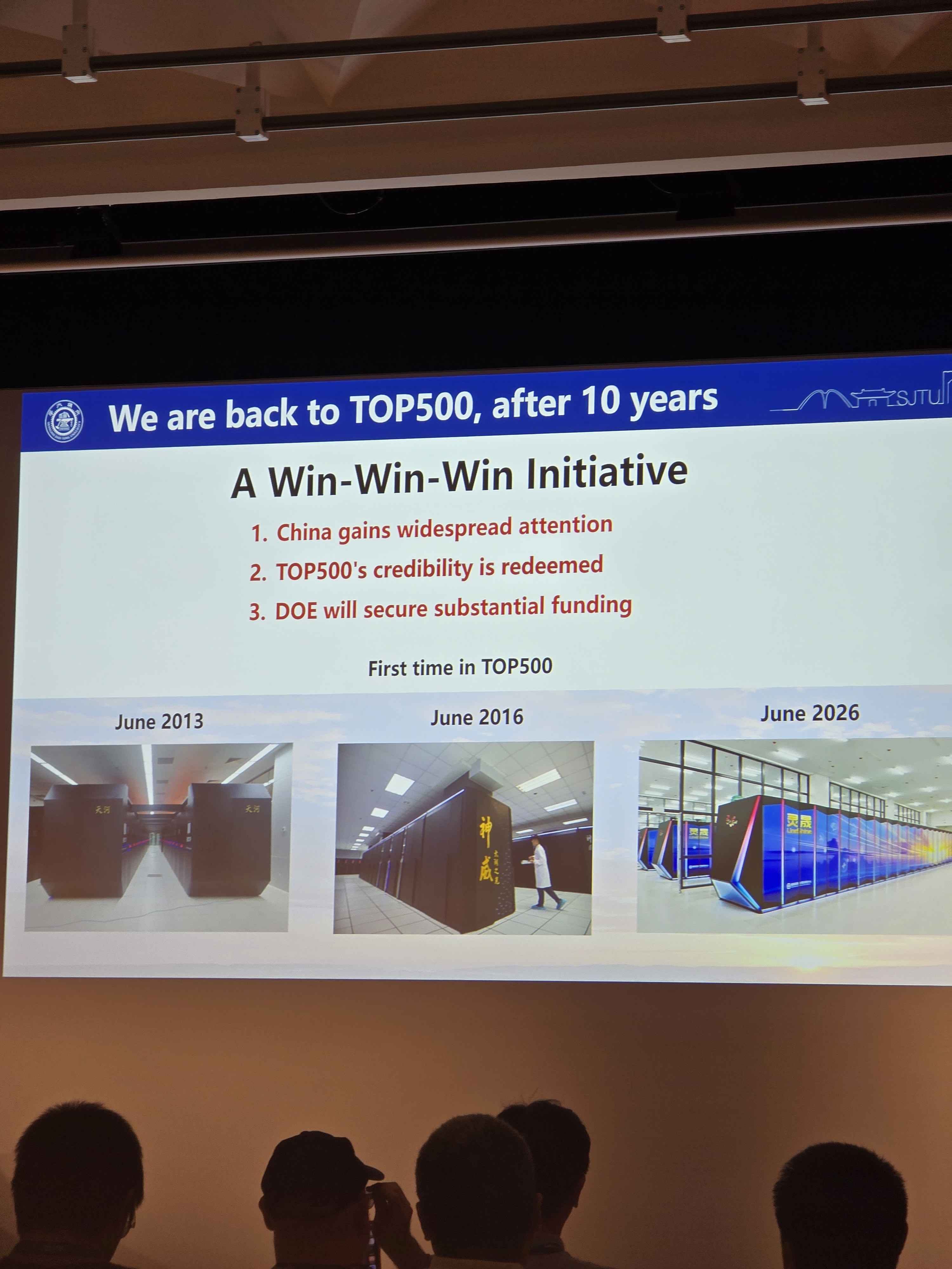
The new number one Supercomputer on the TOP500 list is the LineShine Supercomputer in Shenzhen, China. This is the first Chinese submission to the TOP500 in 9 years and they came in swinging with a massive CPU-only system.
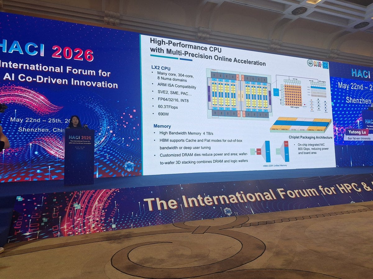
Starting with the specifications of the CPU that powers the LineShine system, the LX2.
The LX2 is an Armv9-compliant CPU with support for SVE2 and SME. Each core has 32 KB of L1 instruction cache and 32 KB of L1 data cache. Physically, the chip is built from two compute dies, with each die containing four 40-core clusters. Two cores are disabled per cluster, leaving 38 active cores per cluster, or 152 active cores per die. Each cluster is backed by 28.5 MB of L2 cache, giving each die 114 MB of L2 and the full LX2 package 304 active cores with 228 MB of total L2 cache.
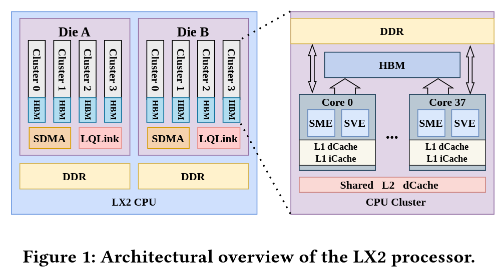
Those 304 cores run at 1.55 GHz and deliver a quoted 60.3 TFLOP/s of FP64 compute at 690 watts per LX2 CPU. The package also includes eight stacks of “high-bandwidth memory,” with 4 GB per stack for 32 GB of on-package high-bandwidth memory and 4 TB/s of bandwidth. However, this memory likely is not conventional HBM, despite being described in similar terms and could be an indigenous Chinese development. Because 32 GB is relatively small for a CPU of this scale, each LX2 is also backed by 256 GB of DDR5 memory that acts as a larger spillover tier.
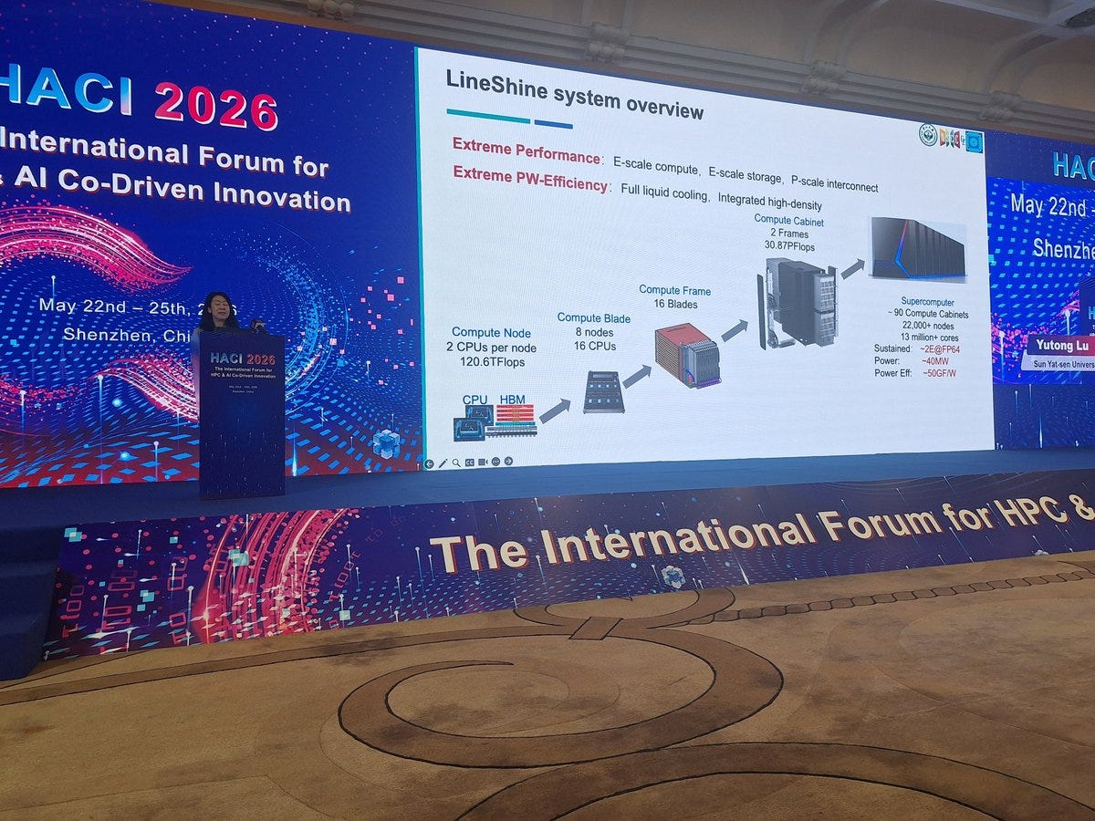
Transitioning from the CPU level to the node level, each node has two LX2 CPUs with 800 Gbps of networking for a total of 1.6Tbps of networking per node. 8 of these nodes are then combined into a compute blade, with 16 compute blades in a compute frame, and 2 frames per compute cabinet. In total the LineShine supercomputer has 90 compute cabinets which means that there are over 22,000 nodes and 13 million CPU cores in the full system.
This puts the LineShine system at a total of 2.198 Exaflops of sustained FP64 (Rmax) out of an on-paper 2.735 Exaflops of FP64 (Rpeak). For this result, the LineShine system pulled 42.22 Megawatts of power for a FP64 efficiency of 52.07 Gigaflops per Watt, which, while it is well behind the leader of 73.282 FP64 Gigaflops per Watt, is very impressive for a CPU only system. And unlike prior Chinese Supercomputers, this system is not just a “LINPACK-special” but is also the number 1 in the HPCG benchmark with a result of 22.004 Petaflops per second beating out El Capitan’s 17.406 Petaflops per second result.
There is a new number 6 system on list, the HPC7 system from Eni in Italy. This is functionally El Capitan, just shrunk down to 30% the size. It is using the same HPE Cray EX4000 platform and AMD Instinct MI300A APUs, which is getting an Rmax of 571.5 Petaflops of FP64 performance out of an Rpeak of 861 Petaflops at 8.735 Megawatts of power consumed. With HPC7, Italy now has more compute listed on the TOP500 than any other country in Europe, despite Germany having Europe’s only Exascale system on the TOP500.
The former number 1 supercomputer, Fugaku, may have been pushed down to number 9 in the TOP500 ranking but it is still a lean, mean, science crunching machine. Despite being 6 years old, Fugaku is still number 3 on the HPCG list, which is a testament to the HPC focused design that Fugaku has, as it is still in the top 3 supercomputers as far as the HPCG list is concerned.
Moving to the Green500, there have been no changes to the Green500’s Top 10 list of most efficient supercomputers. This is the first time in the Green500’s history where there have been no changes to the Top 10 list. However that is not to say that HPC hasn’t gotten more efficient.
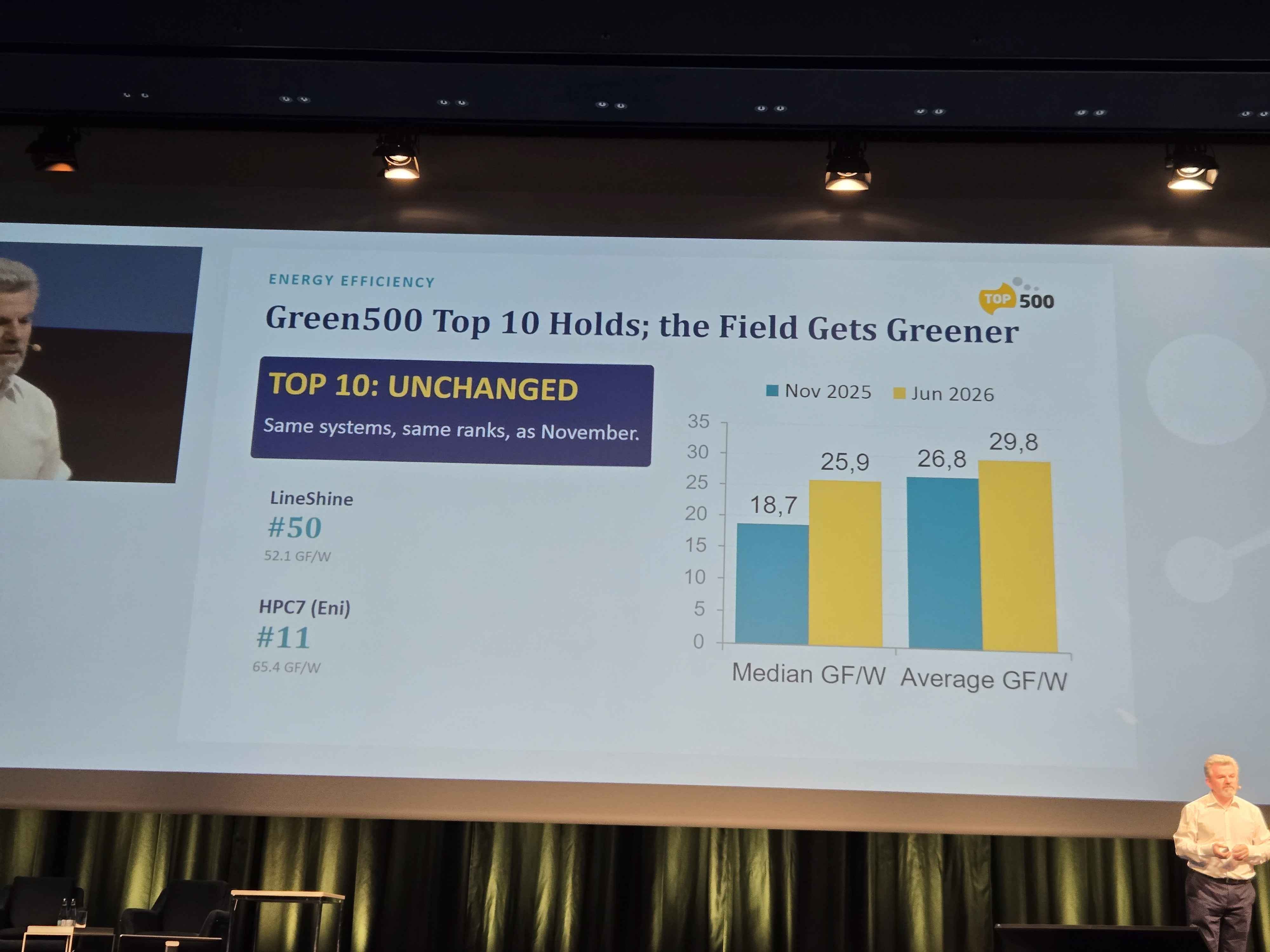
Due to retirements of older systems, the overall field of HPC has gotten more efficient in the past 6 months.
Personally, I wasn’t expecting to see a new number 1 on the TOP500, until either Discovery or Fukagu-Next was brought online. We have known that China has Exascale systems for a while now, but this is the first time that we have seen a China Exascale system on the TOP500.
This does beg the question of if China will also submit TOP500 results for their other exascale systems, Sunway Oceanlight and CNIS, or if they will keep those off of the TOP500 list.
I do wonder if this will cause the US Government to spend more money for large DOE systems and I am not the only one thinking that it could drive more money towards the DOE.
If the submission of LineShine ends up with the DOE getting more funding for more, and larger, supercomputers, then bully for us in the HPC community.
Something that is quite interesting is that Eni, an oil and gas company, has been submitting their systems to the TOP500 and they currently have 2 of the Top 10 systems on the TOP500. Which then begs the question, why aren’t the truly large AI systems, such as xAI’s Colossus 2 with over 550,000 Blackwell GPUs, on the TOP500? Why aren’t these AI companies submitting to the TOP500 to show off their computing prowess? To be honest, I don’t know why. A full HPL run on a supercomputer seems like a good way to stress all of the compute, memory, and networking of the system before declaring it to be operational.
There was one last key piece of news that came out of the TOP500 here at ISC 2026 and that is that the ISC Group will be handing over the TOP500 list to ACM SIGHPC moving forward. This functionally means that now all TOP500 lists will have dedicated DOI numbers which will make referencing specific TOP500 lists easier moving forward.